High resolution ADC based on an oversampled subranging ADC
- Summary
- Abstract
- Description
- Claims
- Application Information
AI Technical Summary
Benefits of technology
Problems solved by technology
Method used
Image

Examples
first embodiment
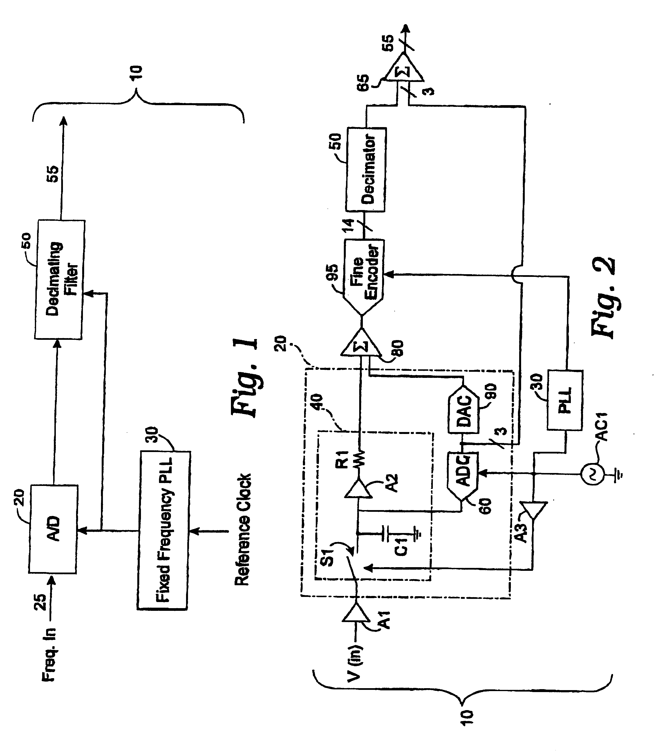
FIG. 1 is a block diagram of the present invention ADC. As shown in FIG. 1 the inventive circuit 10 comprises a front end circuit ADC baseline device 20 for processing 14 bit data at an 80 mega-sample per second (MSPS) data rate with 14 bit dynamic range at a baseline clock rate. A phase-locked loop (PLL) circuit 30 is included for generating the baseline clock rate by multiplying the reference clock frequency by a factor of 8. A decimating filter 50 (decimator) is included to reduce the 80 MSPS data rate of the baseline device 20 to a 10 MSPS data rate so as to achieve 8 times oversampling. This over-sampling allows enhancement of the baseline ADC SNR to achieve the SNR of the final ADC. Hence, the output date rate is 8 times slower than the baseline clock rate and provides output data 55 with 16-bit resolution and 10 MSPS data rate. The input signal 25 drives an input sample and hold circuit, which is further described in FIG. 2.
second embodiment
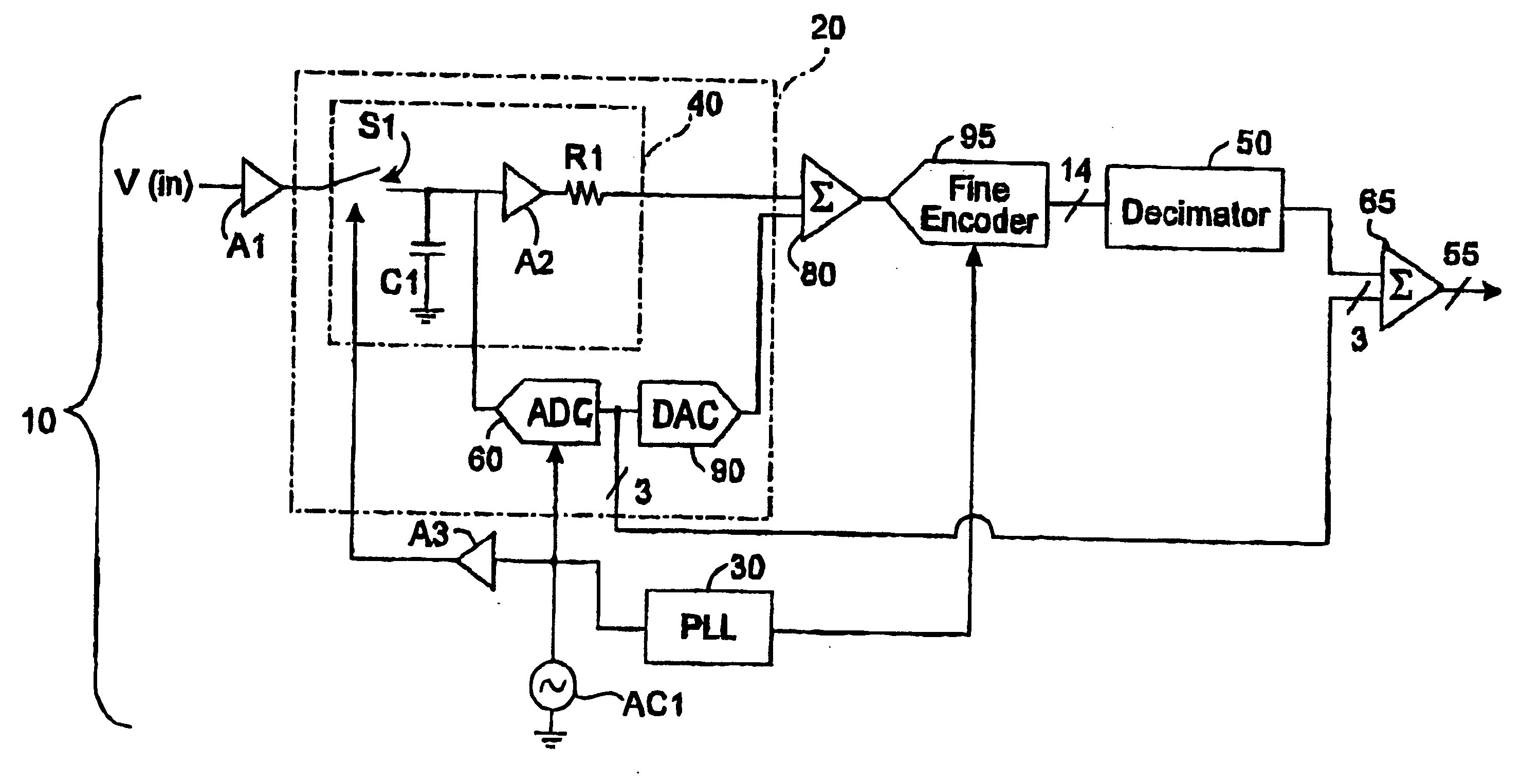
FIG. 2 is a block diagram of the present invention ADC. As shown, a front end 20 provides a band limited sample and hold circuit 40 and runs at a clock rate equal to the final clock rate. The front end 20 provides an input buffer unity amplifier Al feeding the input signal V(in) to the sample and hold circuit 40 comprising a sampling switch S1, as shown, operated at the rate of crystal oscillator AC1, capacitor C1, and resistor R1. R1 is a critical resistor for generating a residue of the input signal. The 3-bit, ADC 60 is driven by crystal oscillator AC1. Summing circuit element (sum node) 80 provides summing of the DAC 90 output signal and the value of the sample during each cycle. The DAC is implemented in CMOS to remove thermal shot noise sources. Fine encoder 95 is preferably a three-step encoder sampling at the baseline sample rate as driven by the PLL circuit 30 at 80 MHz. At the output this signal as decimated through decimating filter 50 is summed with the ADC 60 front-end ...
PUM
 Abstract
Description
Claims
Application Information