Specialized substrates for use in sequential lateral solidification processing

a technology of sequential lateral solidification and substrates, applied in the direction of crystal growth process, transportation and packaging, water-setting substance layered product, etc., can solve the problems of physical distortion, glass that has not been observed, and attempts to achieve commercially viabl

Inactive Publication Date: 2003-06-24
THE TRUSTEES OF COLUMBIA UNIV IN THE CITY OF NEW YORK
View PDF4 Cites 107 Cited by
  • Summary
  • Abstract
  • Description
  • Claims
  • Application Information

AI Technical Summary

Problems solved by technology

While there have been attempts to utilize low thermal conductivity materials, such as porous glass, in connection with sequential lateral solidification for the purpose of enhancing lateral crystal growth, such attempts have not achieved commercially viable results.
For example, when a porous glass layer is used under a silicon film in the sequential lateral solidification process densification, and subsequent physical distortion, of such glass has been observed.

Method used


Image

  • Specialized substrates for use in sequential lateral solidification processing
  • Specialized substrates for use in sequential lateral solidification processing

Examples


Embodiment Construction

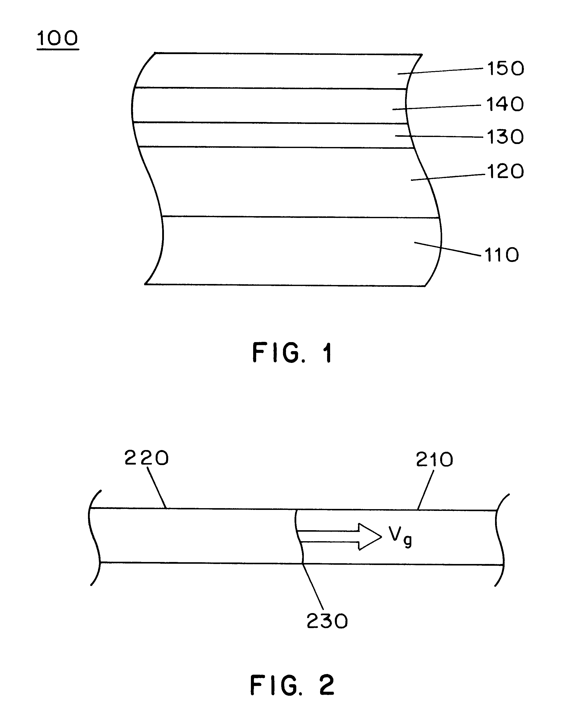
Referring to FIG. 1, a preferred embodiment of the present invention will be described. As shown in FIG. 1, the substrate 100 includes a bulk glass plate layer 110, a low conductivity layer 120, a high conductivity layer 130, a silicon dioxide layer 140, and a semiconducting film layer 150. The multilayer structure of substrate 100 may be fabricated by any combination of thin film formation techniques, such as physical or chemical vapor deposition,,electrochemical deposition, or spin coating.

The low conductivity layer 120 may be porous glass or a polymer film layer. In addition, the layer 120 must have a conductivity which is less than the glass plate 110 and sufficiently thick so that the glass plate layer 110 will not participate when the substrate 100 is used in later processing. Layer 120 will be in the order of 5,000 Angstroms to 2 microns thick.

The high conductivity layer 130 may be a metallic layer such as copper or aluminum. The high conductivity layer must have a conductivi...


PUM

PropertyMeasurementUnit
thickaaaaaaaaaa
thickaaaaaaaaaa
thickaaaaaaaaaa

Abstract

Substrates having modified effective thermal conductivity for use in the sequential lateral solidification process are disclosed. In one arrangement, a substrate includes a glass base layer, a low conductivity layer formed adjacent to a surface of the base layer, a high conductivity layer formed adjacent to the low conductivity layer, a silicon compound layer formed adjacent to the high conductivity layer, and a silicon layer formed on the silicon compound layer. In an alternative arrangement, the substrate includes an internal subsurface melting layer which will act as a heat reservoir during subsequent sequential lateral solidification processing.

Description

I. Field of the Invention.The present invention relates to techniques for processing of semiconductor films, and more particularly to techniques for processing semiconductor films on glass or other substrates.II. Description of the Related Art.Techniques for fabricating large grained single crystal or polycrystalline silicon thin films using sequential lateral solidification are known in the art. For example, in U.S. patent application Ser. No. 09 / 390,537, the contents of which are incorporated by reference herein and which application is assigned to the common assignee of the present application, particularly advantageous apparatus and methods for growing large grained polycrystalline or single crystal silicon structures using energy-controllable laser pulses and small-scale translation of a silicon sample to implement sequential lateral solidification are disclosed. Using the sequential lateral solidification technique, low defect density crystalline silicon films can be produced ...

Claims


Application Information

Patent Timeline
Patent Type & Authority Patents(United States)
IPC IPC(8): C30B11/00H01L21/20
CPCC30B11/00C30B29/06H01L21/2026Y10T428/256Y10T428/12674Y10T428/252Y10T428/249969H01L21/02686H01L21/02422H01L21/02488H01L21/02491H01L21/02532H01L21/02505H01L21/0254H01L21/02546H01L21/02667
Inventor IM, JAMES S.
Owner THE TRUSTEES OF COLUMBIA UNIV IN THE CITY OF NEW YORK
Why Eureka
Try Eureka