Dielectric element and method for fabricating the same

a technology of dielectric elements and dielectric elements, which is applied in the field of dielectric elements, can solve the problems of deteriorating electrical characteristics of dielectric elements, affecting the degree of integration of ic circuits using pt, and taking a long time to process p

Inactive Publication Date: 2003-07-22
TOKYO OHKA KOGYO CO LTD
View PDF6 Cites 14 Cited by
  • Summary
  • Abstract
  • Description
  • Claims
  • Application Information

AI Technical Summary

Problems solved by technology

However, the mass-production processing limit, i.e., etching performance, of a Pt electrode is about 0.8 .mu.m at present, and the electrode after the processing is likely to have a tapered or trapezoidal shape.
Thus, an increase in the degree of integration of IC circuits using Pt still has problems to be solved.
Moreover, since it is difficult to perform etching Pt by a chemical reaction with a halogen gas, Pt is generally processed physically by a sputtering method and the like.
However, the damage caused to a dielectric layer during such a physical processing method deteriorates electrical characteristics of the dielectric element.
Furthermore, it takes a long time to process Pt, and Pt residues generated during the processing may be adhered to an inner wall of a processing chamber, thereby causing contamination.
It also describes that as Pt is mostly processed by physical sputtering method, an etched-away residue or product may be adhered to the processed Pt electro

Method used


Image

  • Dielectric element and method for fabricating the same
  • Dielectric element and method for fabricating the same
  • Dielectric element and method for fabricating the same

Examples


example 1

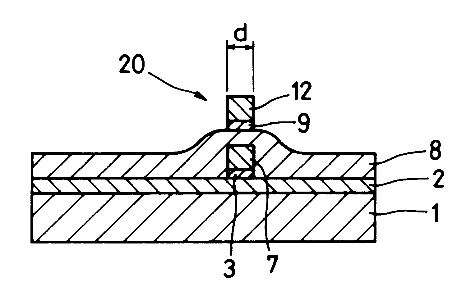
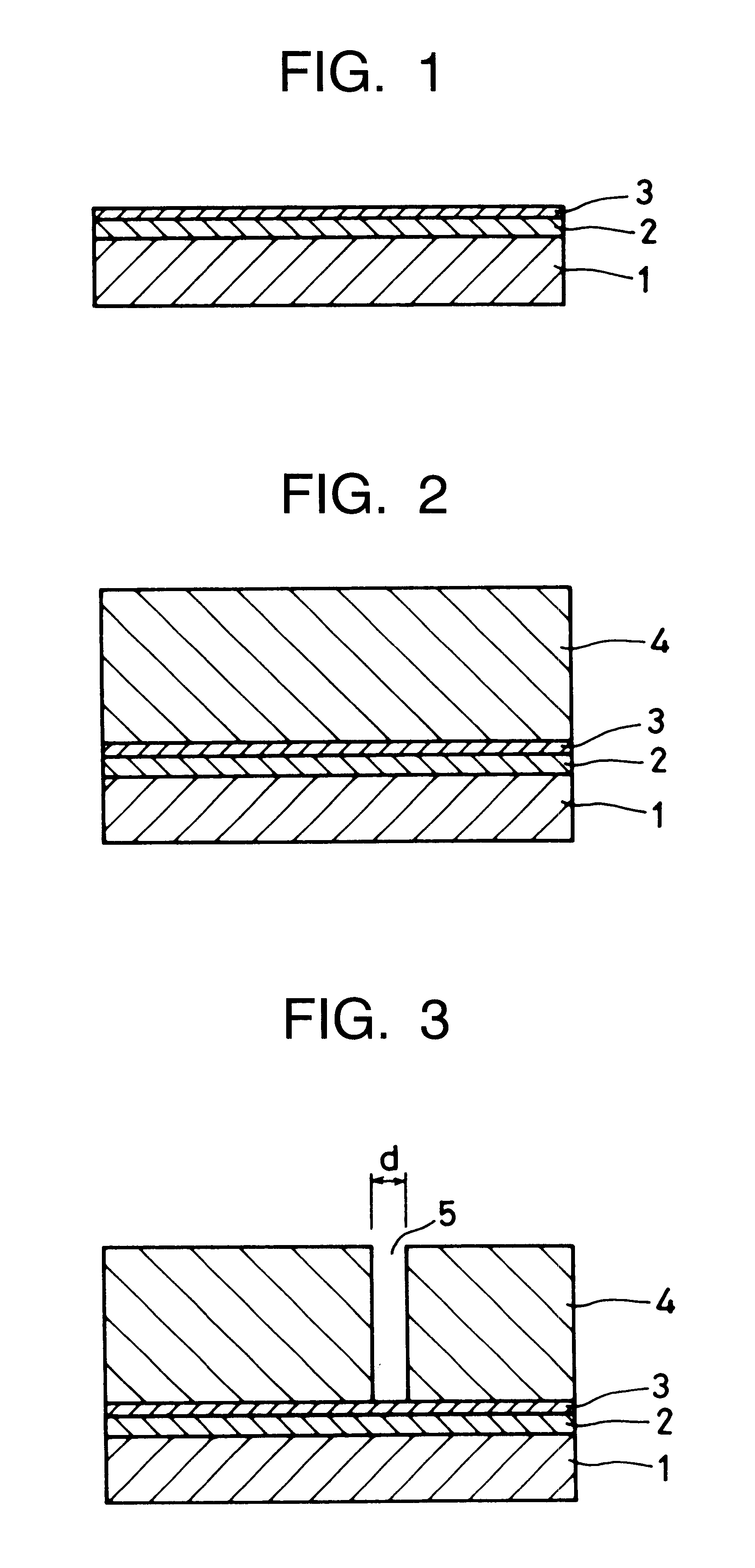
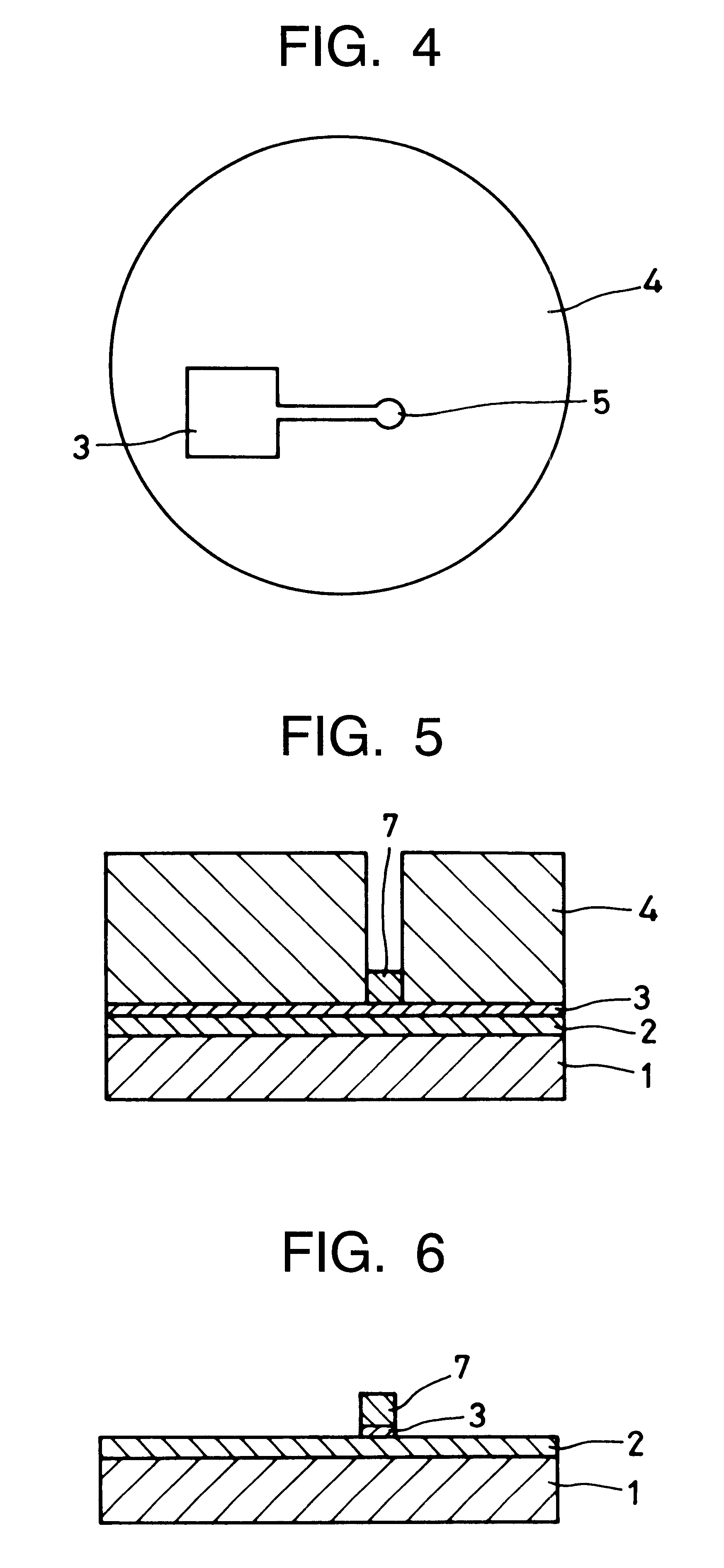
As illustrated in FIG. 1, an Ru layer 3 with a thickness of 50 nm was formed by sputtering on a Si substrate 1 of a 6-inch diameter on which an SiO.sub.2 film 2 having a thickness of 100 nm was provided.

Then, as illustrated in FIG. 2, a photoresist layer 4 having a thickness of 800 nm was formed onto the surface of the Ru layer 3 entirely using i-line positive photoresist coating solution "TDMR-AR80" (product of Tokyo Ohka Kogyo Co., Ltd.). The photoresist layer 4 was selectively exposed through a mask (not shown) for an exposure time of 200 msec. As the exposure apparatus, the i-line stepper "NSR-2205i14E" (Nikon Corp.) was used.

After the exposure, a development process was performed using 2.38 wt % of tetramethylammonium hydroxide (TMAH) aqueous solution. Next, the photoresist layer 4 was washed with water, dried, and then subjected to a vacuum UV process and a hard bake process at a temperature of 180.degree. C. for 3 minutes. As a result, a hole pattern 5 (FIG. 3) having a diame...


PUM


Abstract

It is disclosed a dielectric element comprising a lower electrode, a dielectric layer, and an upper electrode which are provided on a substrate, in which at least one of the electrodes is a Pt layer, a Ru layer is used as a base layer for the Pt layer. In the fabrication of the dielectric element, the Pt layer is formed by electroplating, a photoresist pattern is used as a plating mask, and an Ru layer is formed as a seed layer. The present invention makes it possible to provide a dielectric element using Pt as an electrode material, that is capable of easily forming a Pt electrode having excellent electrical characteristics without generating voids or seams, that is capable of forming a fine pattern, and that does not occur contamination in a processing chamber, and a method for fabricating a dielectric element of having the characteristics mentioned above.

Description

1. Field of the InventionThe present invention relates to a dielectric element having a lower electrode, a dielectric layer, and an upper electrode in which Pt is used as an electrode material, and a method for fabricating such a dielectric element.2. Description of Relevant ArtIn recent years, attempts have been made actively to apply a dielectric element fabricated by using a high dielectric material such as BTO, STO or BST, or by using a ferroelectric material such as SBT, SBTN or PZT to a next-generation highly integrated DRAM or non-volatile memory.Each of the aforementioned dielectric materials is made of plural metal oxides. Since a process for forming a dielectric layer is performed in an oxidative atmosphere, it is desirable to use a conductive material as an electrode material for a dielectric element that is not likely to be oxidized, or exhibits a conductivity even when it is oxidized.Those conductive materials include metals such as Pt, Ir, Ru, Rh, Re, Os, and Au, and o...

Claims


Application Information

Patent Timeline
IPC IPC(8): H01L21/02H01L27/10H01B3/12H01L21/8246H01L27/105H01L27/108
CPCH01L28/75H01L28/55Y10S438/957H10B12/00
Inventor HASHIMOTO, AKIRASATO, YOSHIMIKAWAKAMI, ATSUSHIKOBARI, HIDEYANAKAJIMA, TETSUYA
Owner TOKYO OHKA KOGYO CO LTD
Why Eureka
Try Eureka