

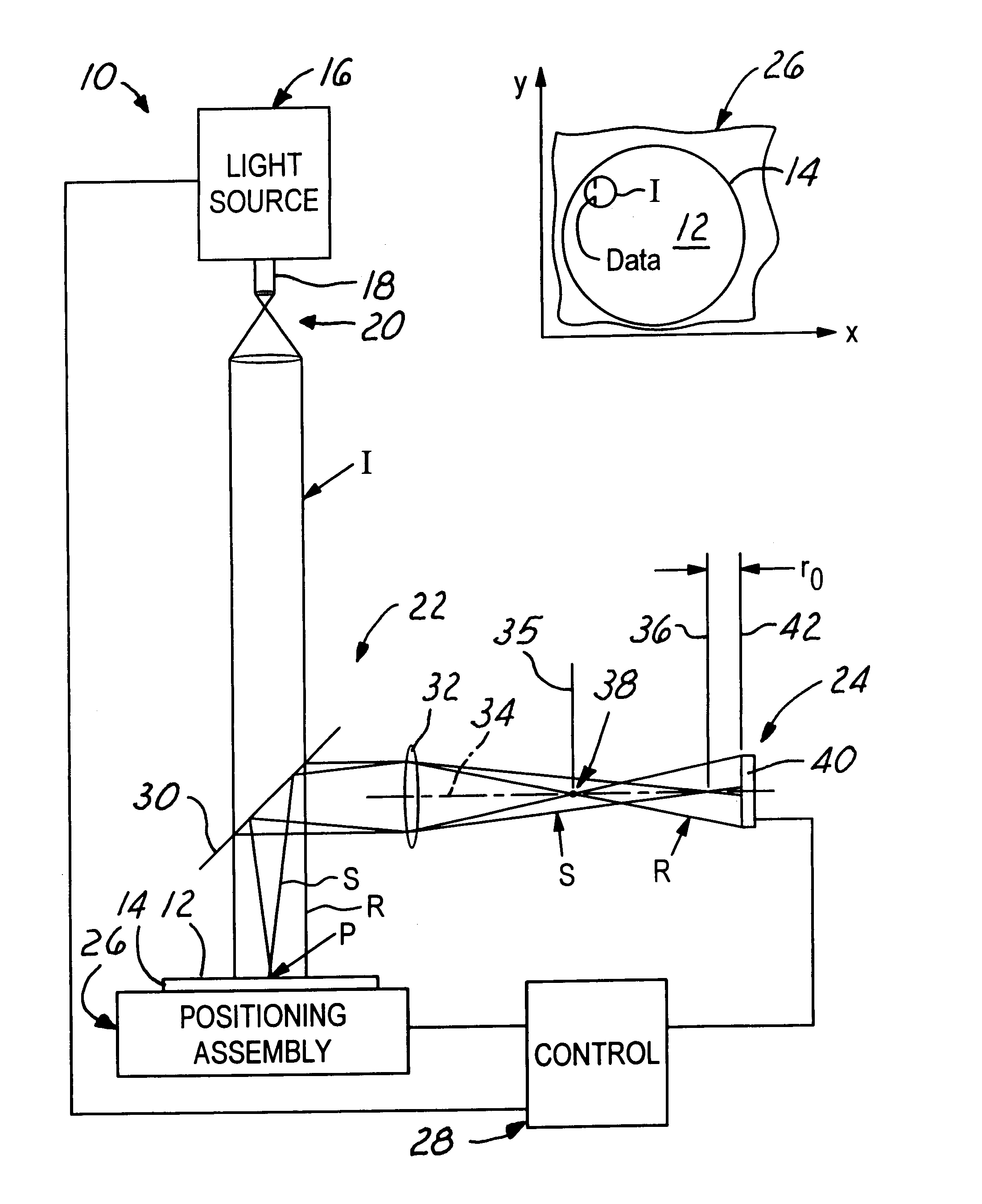
Holographic scatterometer for detection and analysis of wafer surface deposits
a holographic scatterometer and wafer surface technology, applied in the field of optical inspection instruments, can solve the problems of inability to perform in-process surface inspection, and insufficient resolution and accuracy of optical microscopes in general
- Summary
- Abstract
- Description
- Claims
- Application Information
AI Technical Summary
Benefits of technology
Problems solved by technology
Method used
Image

Examples
Embodiment Construction
Let A equal the intensity of a single pixel corresponding to a phase difference between the signal beam S and the reference beam R, namely, .theta.; B equal to the intensity of another pixel (in the same line) corresponding to .theta.+90.degree.; C equal to the intensity of yet another pixel (in the same line) corresponding to .theta.+180.degree.; and D equal to the intensity of still another pixel (in the same line) corresponding to .theta.+270.degree.. Evaluating equation (9) yields:
Ipro(m)=[(A-C).sup.2 -(B-D).sup.2 ].sup.1 / 2
In the TDI mode of operation, a "constellation" of 4 points gets brighter and brighter when a particle P is present on surface 12. Two phases may also be used rather than four.
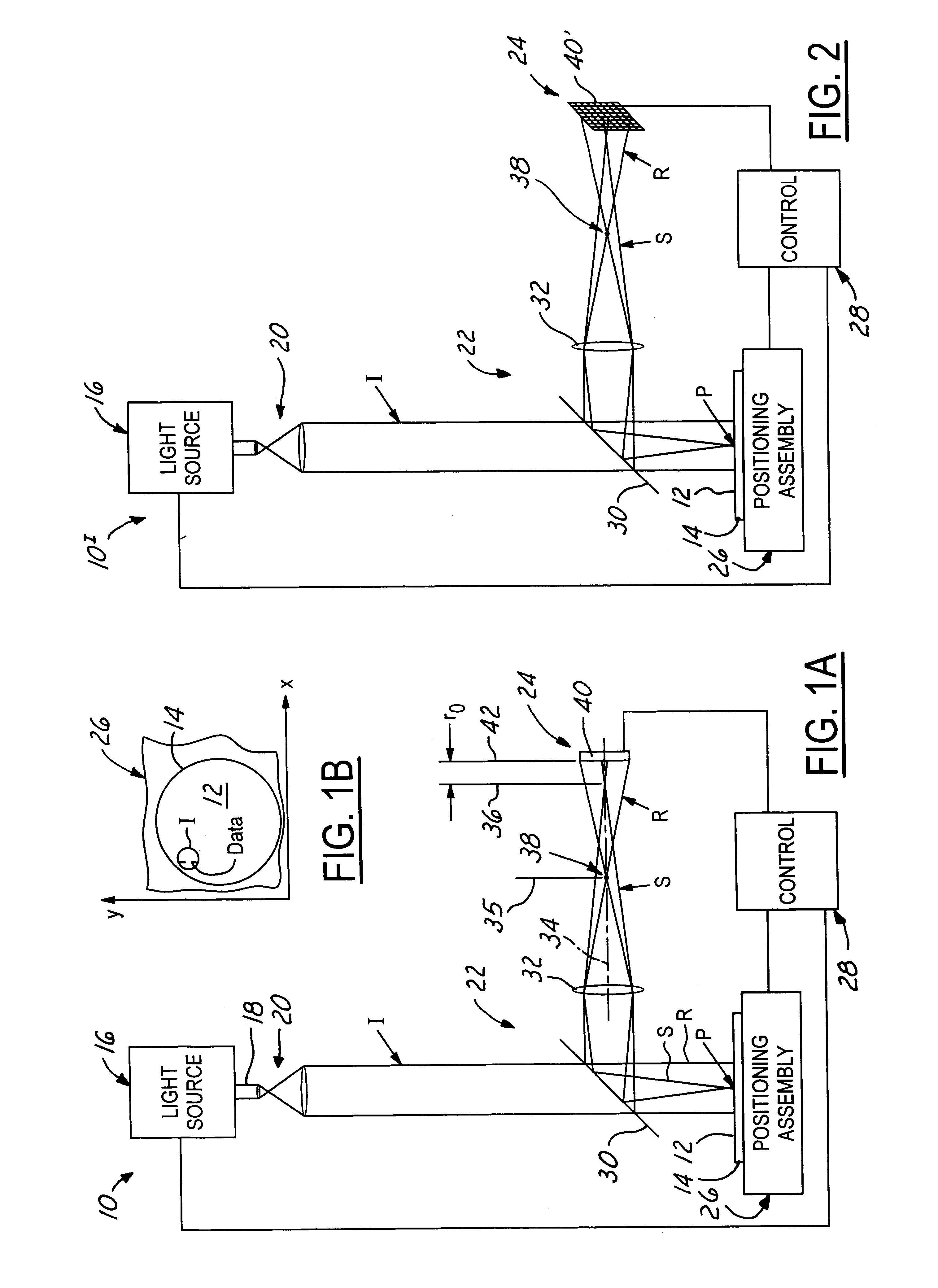
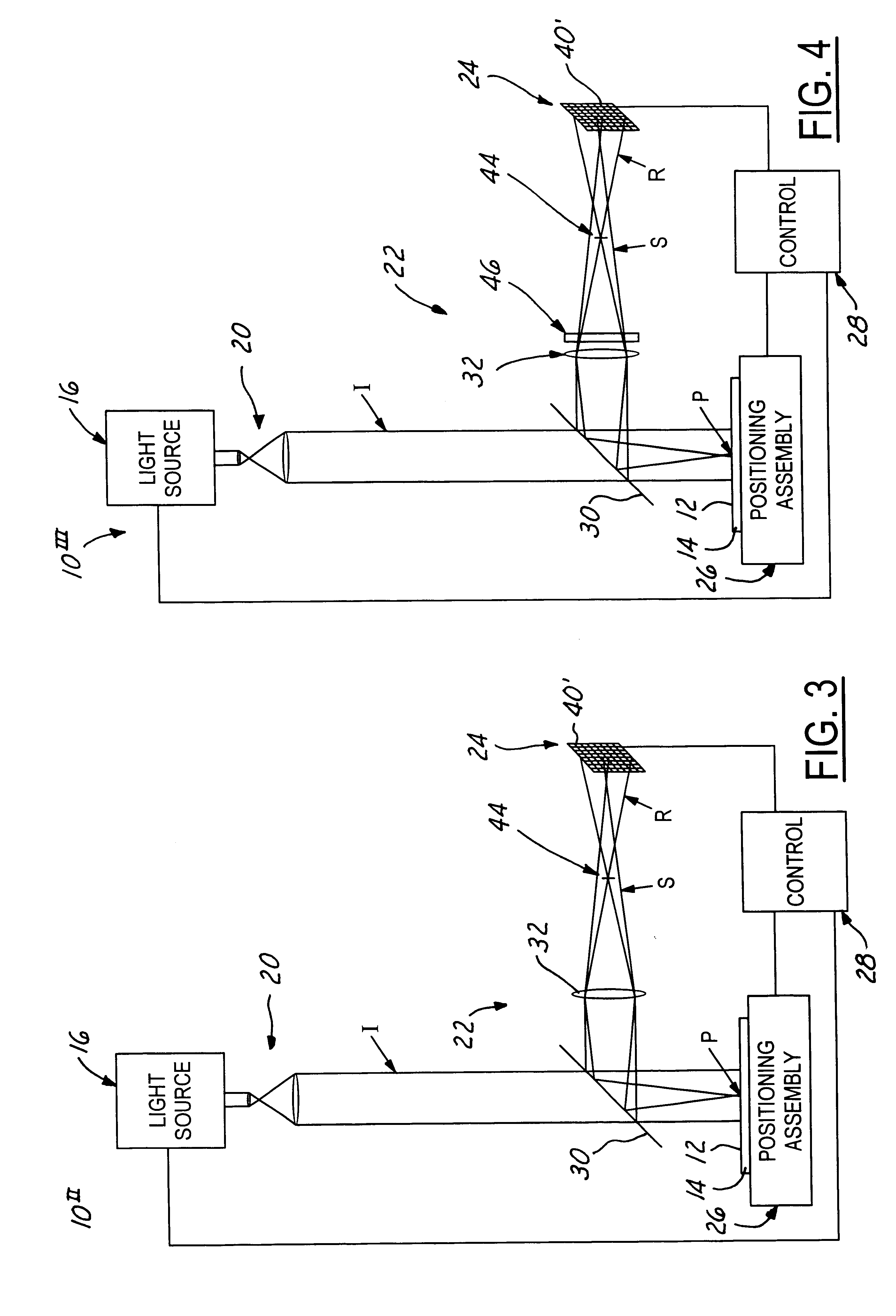
FIG. 9 shows an alternate, preferred, arrangement for the optical assembly 22 illustrated in FIGS. 1A, and 2-8. In particular, assembly 22' still includes beam splitter 30 and lens 32, but in addition further includes reflecting surfaces 70, 72, and 74. The advantage provided by assembly...
PUM
| Property | Measurement | Unit |
|---|---|---|
| angle | aaaaa | aaaaa |
| diameter | aaaaa | aaaaa |
| particle size | aaaaa | aaaaa |
Abstract
Description
Claims
Application Information