Semiconductor device manufacturing method, heat treatment apparatus, and heat treatment method

a technology of semiconductor devices and manufacturing methods, applied in semiconductor devices, electrical devices, transistors, etc., can solve the problems of difficult laser annealing in a mass production process, unsatisfactory controllability and reproducibility, and reduced activation efficiency

Inactive Publication Date: 2003-07-29
SEMICON ENERGY LAB CO LTD
View PDF11 Cites 102 Cited by
  • Summary
  • Abstract
  • Description
  • Claims
  • Application Information

AI Technical Summary

Benefits of technology

In order to attain the above objects, the present invention provides a method of heat treatment for performing gettering and activation on a semiconductor film formed on a low heat resistant substrate such as a glass substrate in a short period of time without causing deformation or other heat-induced damage to the substrate, as well as a heat treatment apparatus for carrying out the method.
The treatment object is kept in the coolant and is irradiated several times by radiation from the lamp light source such that the treatment object holds the temperature to its highest, 600 to 800.degree. C., for 30 to 600 seconds. In this way., the treatment object can be heated efficiently, completing the heat treatment. The wavelength of the electromagnetic wave radiated from the lamp light source is matched to the absorption band of the treatment object for selective heating so that the treatment object alone is heated. Specifically, a semiconductor film formed on a glass substrate having a distortion point of 700.degree. C. or lower is heated.

Problems solved by technology

Laser annealing melts a semiconductor film and is unsatisfactory in controllability and reproducibility, which makes it difficult to employ laser annealing in a mass production process.
On the other hand, furnace annealing is suitable for a mass production process since it treats in batches but its activation efficiency decreases as the process temperature becomes low to prolong the treatment time, which is a problem.
However, the reaction is of nonequilibrium one and the crystals formed therefore have small grain size and many defects.
Furthermore, the direct control factors are effective only for limited ranges.
However, this method leaves the metal element in the semiconductor film crystallized and often needs gettering.
Then, a furnace annealing apparatus, which treats in batches, would not be helpful in improving the production efficiency.
If the furnace annealing apparatus is enlarged, current consumption is increased for heating the large capacity furnace, not to mention it needs larger installment area.
However, short heating time means high heating temperature while a temperature exceeding the distortion point of glass, or even its softening point, is required in order to obtain desired effects in activation and gettering.
When the heat treatment is conducted at higher temperature, the rate the metal element diffuses is raised but effective gettering of the metal element cannot be expected.

Method used


Image

  • Semiconductor device manufacturing method, heat treatment apparatus, and heat treatment method
  • Semiconductor device manufacturing method, heat treatment apparatus, and heat treatment method
  • Semiconductor device manufacturing method, heat treatment apparatus, and heat treatment method

Examples


embodiment 1

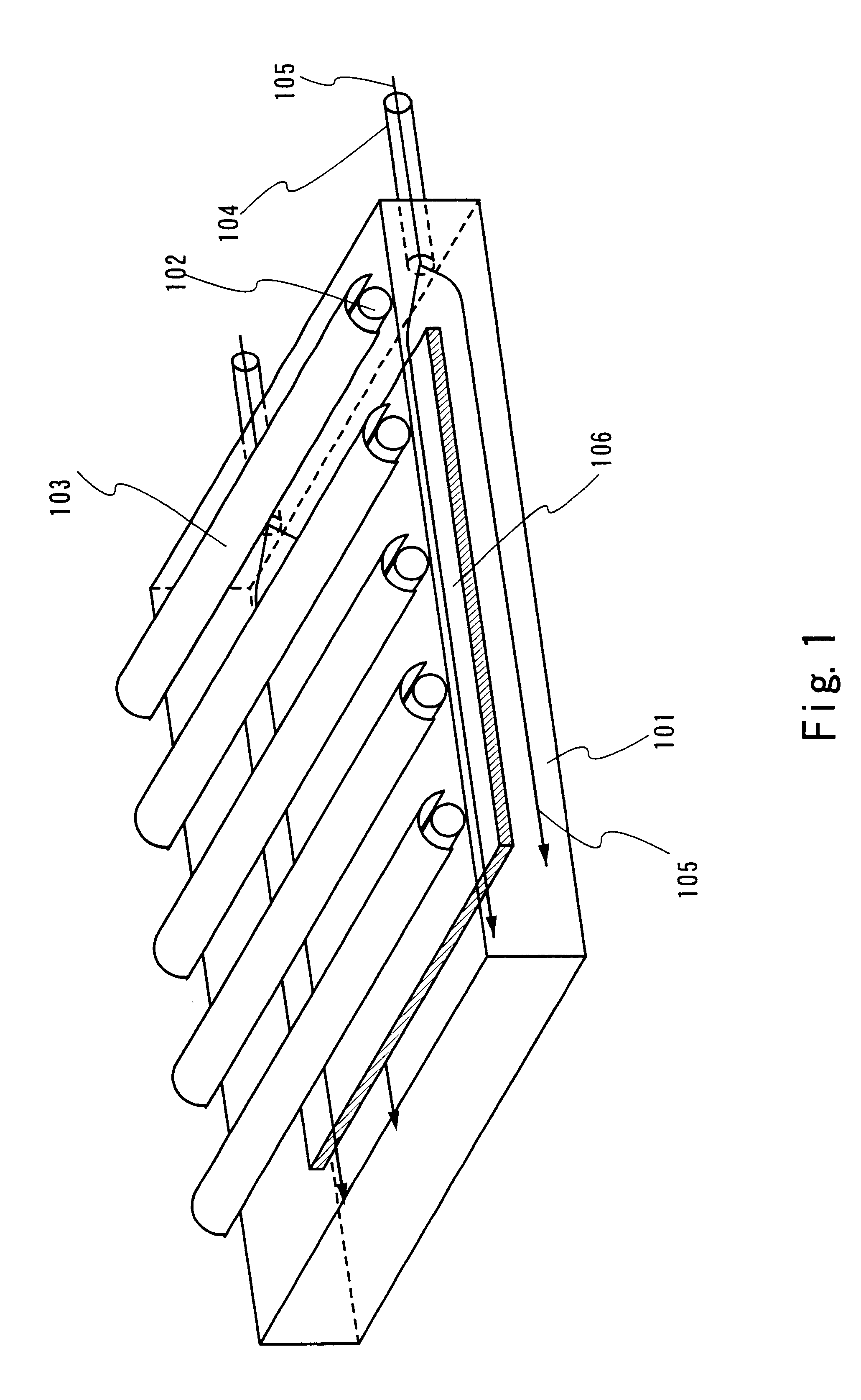
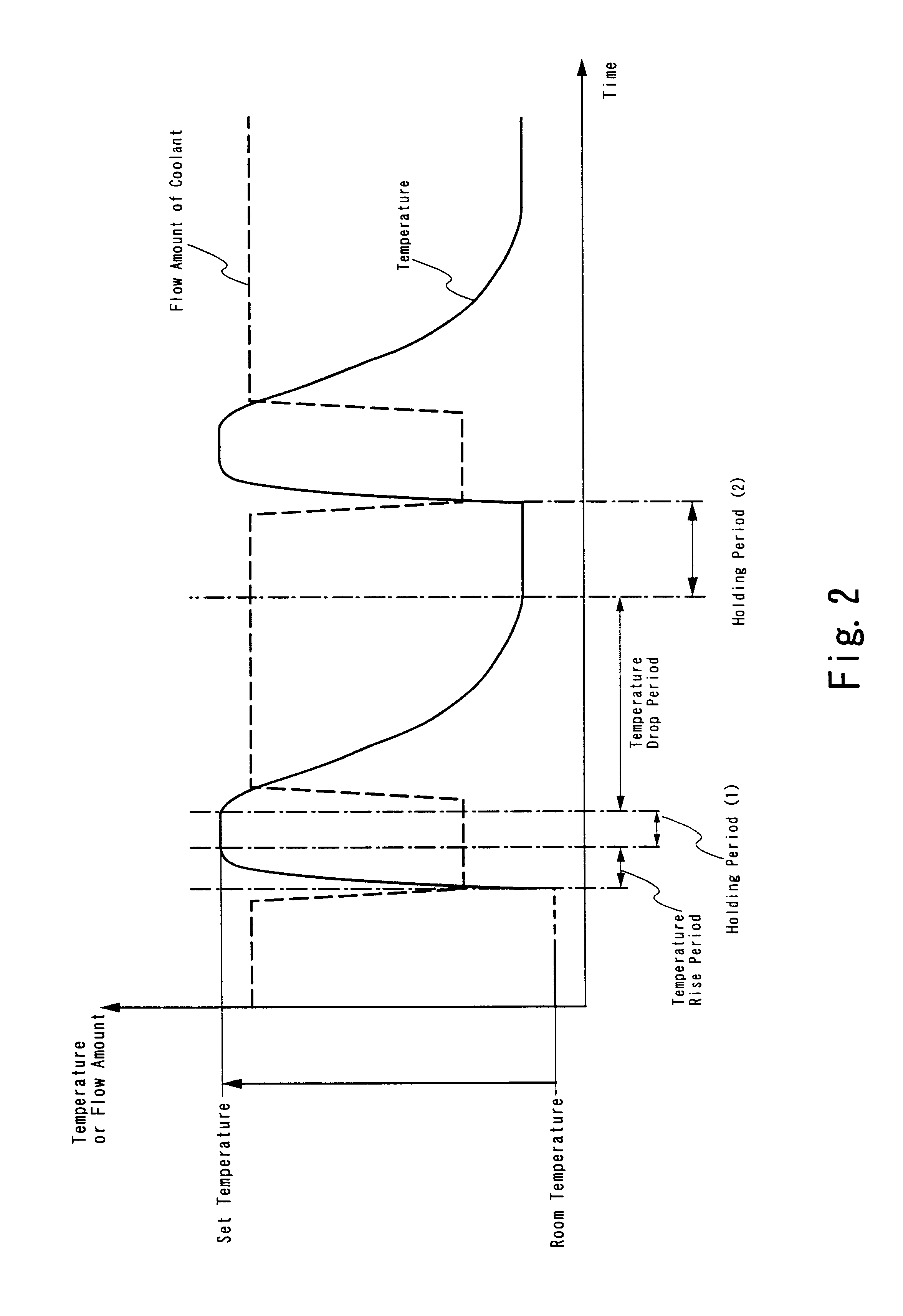
FIG. 5 shows the structure of a single wafer type heat treatment apparatus as an example of a heat treatment apparatus of the present invention. A processing chamber 301 is formed of quartz and is surrounded by water-cool type cooling means 305. A lamp light source 302 has a reflective plate 303 so that pulsative radiation diffuses over a treatment object 317 efficiently. When a rod-like halogen lamp is used, a plurality of lamps are set as shown in FIG. 5 to irradiate the treatment object 317 with pulsative radiation of uniform intensity. Radiation (including a wavelength of 0.5 .mu.m to 3 .mu.m, for example) is made to pulsate by a light source control unit 304.

Nitrogen gas is supplied as a coolant to the processing chamber 301 from a coolant supply source 306. The amount of nitrogen gas to be supplied to the processing chamber 301 can be controlled by flow rate controlling means 307. The coolant supplied to the processing chamber is then discharged from an outlet 311 so that the ...

embodiment 2

As an example of a heat treatment apparatus of the present invention, the structure of an inline type heat treatment apparatus that corresponds to a substrate having a large area is shown in FIG. 16. A processing chamber 1301 is formed of quartz and is surrounded by water-cool type cooling means 1305. A lamp light source 1302 has a reflective plate so that an optical lens 1324 condenses light to irradiate a treatment object. A rod-like halogen lamp is used in a lamp light source 1302, and a cylindrical lens is used as the optical lens 1324, thereby being capable of irradiating the treatment object with a linear light. A lamp light source is lit and made to pulsate by a light source control unit 1304.

Nitrogen gas or helium gas is supplied as a coolant to the processing chamber 1301 from a coolant supply source 1306. The amount of nitrogen gas to be supplied to the processing chamber 1301 can be controlled by a flow rate controlling means 1307. The coolant supplied to the processing c...

embodiment 3

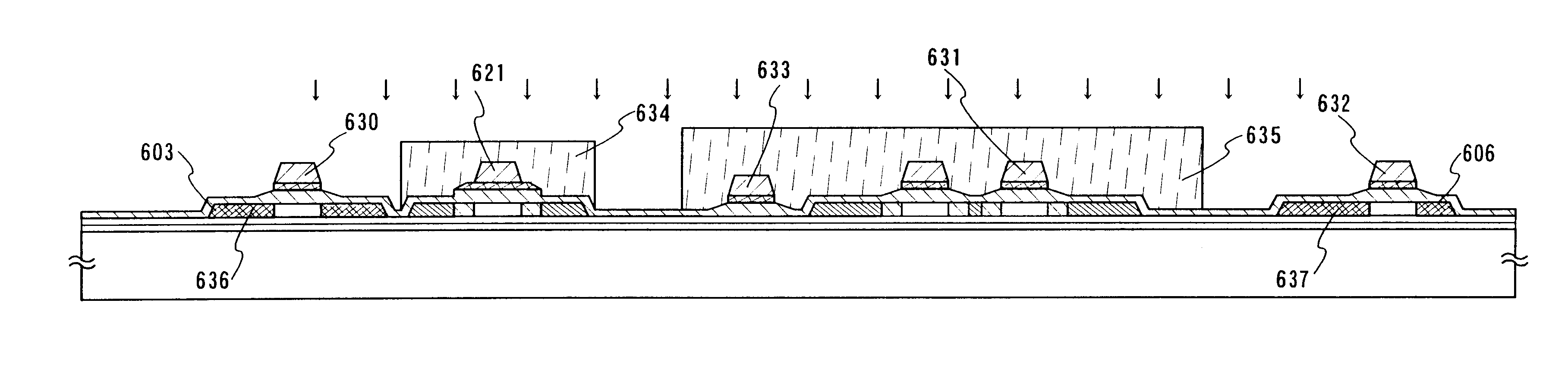
An example of a method of manufacturing TFTs using the present invention will be described with reference to FIGS. 7A to 7F. In FIG. 7A, a crystalline semiconductor film mainly containing silicon is formed on a light transmissive substrate 501 formed of alminoborosilicate glass or barium borosilicate glass. The crystalline semiconductor film is obtained by crystallizing an amorphous semiconductor film through laser annealing. Instead, the heat treatment apparatus described in Embodiment 1 or Embodiment 2 may be used to crystallize an amorphous semiconductor film through pulsative radiation. The crystalline semiconductor film formed has a thickness of 25 to 80 nm. To manufacture TFTs, the crystalline semiconductor film is etched and divided into films having given sizes for element separation. Thus formed are island-like semiconductor films 503 to 505. A first insulating film 502 with a thickness of 50 to 200 nm is formed between the substrate 501 and the semiconductor films. The fir...


PUM

PropertyMeasurementUnit
timeaaaaaaaaaa
temperatureaaaaaaaaaa

Abstract

For manufacture of a semiconductor device using a low heat resistant substrate such as a glass substrate, a method of heat treatment for activating an impurity element that is used to dope a semiconductor film and for performing gettering on the semiconductor film in a short period of time without deforming the substrate, is provided. Also provided is a heat treatment apparatus for carrying out the above heat treatment. The heat treatment method of the present invention involves irradiating an object with light emitted from a lamp light source, and is characterized in that the lamp light source emits light for 0.1 to 20 seconds at a time and that light from the lamp light source irradiates the object several times. The method is also characterized in that the irradiated region is subjected to pulsating light from the lamp light source such that the irradiated region holds the temperature to its highest for 0.5 to 5 seconds. The method is also characterized in that the amount of coolant to be supplied is increased or reduced in accordance with blinking of the lamp light source to enhance the effect of the heat treatment on the semiconductor film and to prevent a heat-induced damage to the substrate.

Description

1. Field of the InventionThe present invention relates to a semiconductor device manufacturing method, a heat treatment apparatus, and a heat treatment method using the apparatus. Specifically, the invention relates to a heat treatment method and a heat treatment apparatus for crystallizing an amorphous semiconductor film, for recrystallizing and activating a semiconductor film that has been brought back to an amorphous state by ion implantation or ion doping, and for gettering of a metal element remaining in the semiconductor film. The invention also relates to a semiconductor device manufacturing method using this heat treatment method.2. Description of the Related ArtHaving silicon as its main ingredient, a crystalline semiconductor film formed at a process temperature of 600.degree. C. or lower is often called low temperature polysilicon. The primal use of this crystalline semiconductor film is of as an active layer for forming a channel formation region, a source or drain regio...

Claims


Application Information

Patent Timeline
Patent Type & Authority Patents(United States)
IPC IPC(8): H01L21/20H01L29/786H01L21/336H01L21/02H01L29/66H01L21/324
CPCH01L21/2022H01L21/2026H01L21/324H01L29/66757H01L29/78621H01L29/78624H01L27/1277H01L21/0262H01L21/02686H01L21/02678H01L21/02422H01L21/02488H01L21/02532H01L21/02672H01L21/02691
Inventor DAIRIKI, KOJI
Owner SEMICON ENERGY LAB CO LTD
Why Eureka
Try Eureka