

Apparatus and method for processing a substrate
a substrate surface and apparatus technology, applied in the direction of non-linear optics, cleaning using liquids, instruments, etc., can solve the problems of inability to produce active oxygen in the vicinity of the substrate surface, and inability to decompose ultraviolet light rays. , to achieve the effect of reducing the capacity of activating organic substances on the substrate surface, reducing the capacity of substrate surface activation, and reducing the capacity of substrate surfa
- Summary
- Abstract
- Description
- Claims
- Application Information
AI Technical Summary
Benefits of technology
Problems solved by technology
Method used
Image

Examples
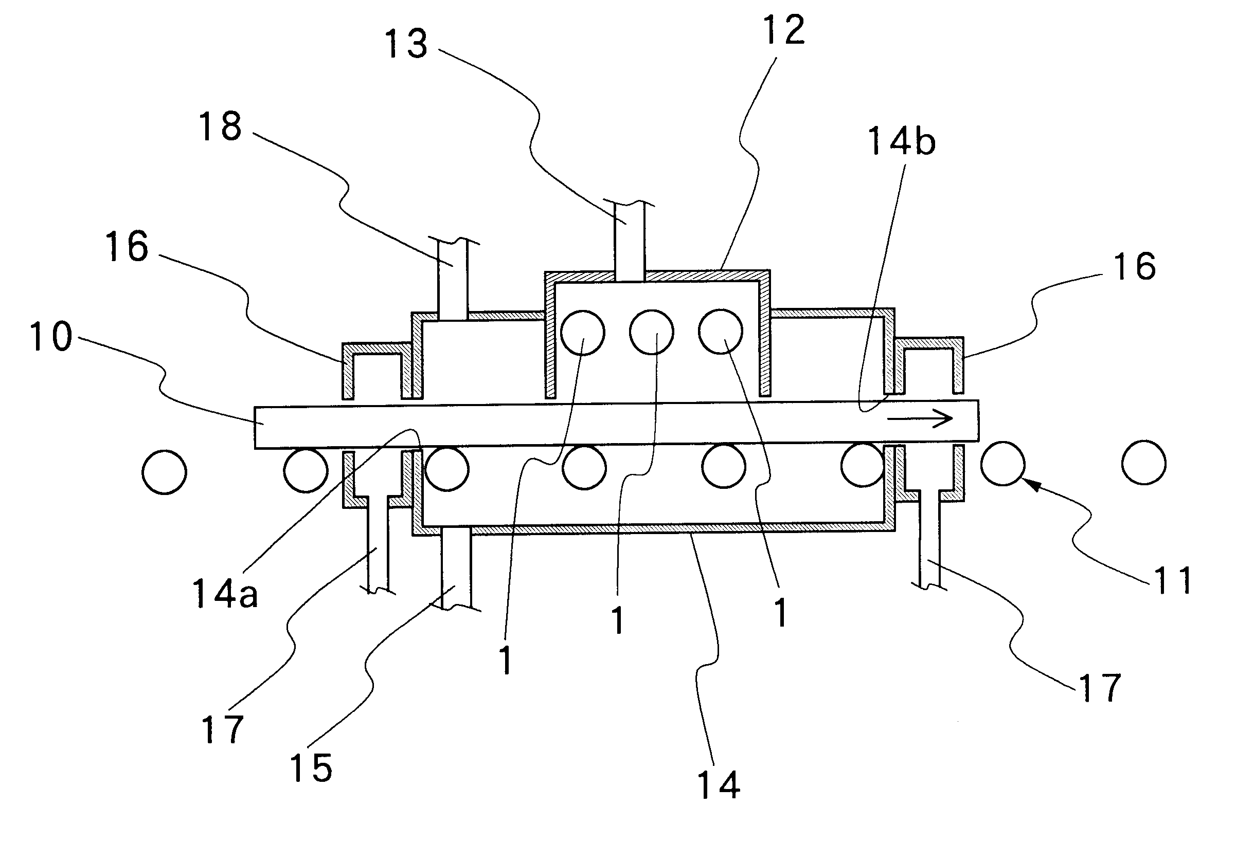
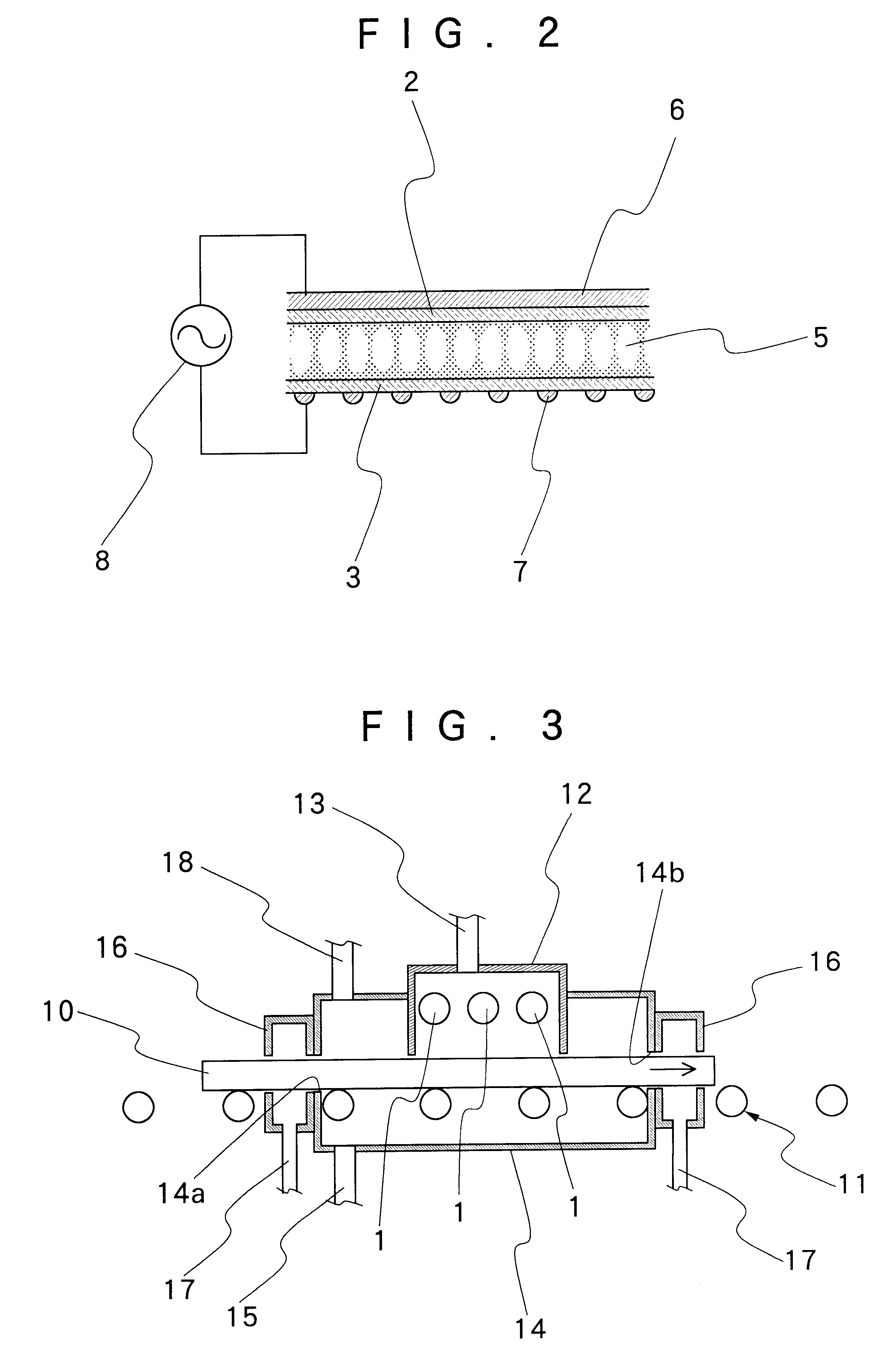
first embodiment
In the case of the first embodiment described above, the lamp house is connected to the lower chamber. However, for the sake of simplification in construction, it may be arranged, for example, as shown in FIG. 5. In the embodiment of FIG. 5, a lamp house 112 is arranged to completely cover or enshroud discharge lamps 1. In this case, on the side which faces a substrate 10, the lamp house 112 is provided is with a window 112a which is fitted with a pane of glass which is highly transmissive of ultraviolet light, 11 such as synthetic quartz glass or the like. With the lamp house 112 of this construction, the inert gas is sealed in the lamp house 112 and not allowed to escape to the outside. Accordingly, in this case, there is no necessity for constantly feeding an inert gas to the lamp house 112 as long as a predetermined amount of inert gas is sealed therein.
Shown in FIG. 6 are results of wettability improving experiments using the apparatus of FIG. 5 and changing the nature of a fee...
fourth embodiment
Illustrated in FIG. 8 is the present invention. In this embodiment, a boundary is provided across an opening at the lower end of the lamp house 212 which is projected into the chamber 214, drawing a border between a dry nitrogen gas atmosphere in the lamp house 212 and a moistened inert gas atmosphere in the chamber 214. The boundary is formed by the use of a partition plate 202 of a predetermined thickness. The partition plate 202 is constituted, for example, by a plate of honeycomb or grid-like structure which contains a multitude of fine passages across its thickness and in its entire surface areas. Further, the partition plate is coated with a reflecting film, including inner surfaces of fine passages.
In this case, the dry nitrogen gas in the lamp house 212 is maintained at a pressure level slightly higher than a gas pressure within the chamber 214. Therefore, a border is defined between the dry nitrogen gas atmosphere in the lamp house 212 and the moistened inert gas atmosphere...
PUM
| Property | Measurement | Unit |
|---|---|---|
| wavelength distribution | aaaaa | aaaaa |
| wavelength distribution | aaaaa | aaaaa |
| wavelength | aaaaa | aaaaa |
Abstract
Description
Claims
Application Information