
Method of producing silica micro-structures from x-ray lithography of SOG materials

Inactive Publication Date: 2004-03-30
LOUISIANA TECH UNIV RES FOUND A DIV OF LOUISIANA TECH UNIV FOUND
View PDF10 Cites 2 Cited by
  • Summary
  • Abstract
  • Description
  • Claims
  • Application Information

AI Technical Summary

Benefits of technology

The present invention provides a lithographic method for producing high aspect ratio silica micro-structures. The method comprises providing a carrier substrate with a confinement boundary placed on the carrier substrate. The SOG material is then placed within the confinement boundary and soft baked at a temperatu

Problems solved by technology

However, all these methods require high temperatures and / or vacuum techniques, and are generally suitable only for thin films.
Thicker prior art SOG films on silicon wafers are prone to fail by cracking.
The development of cracks in thick SOG films can be attributed to shrinkage during drying.
Cracking of the film occurs because as shrinkage takes place, the SOG continues to adhere to the substrate, resulting in a buildup of tensile stress within the film.
In thick films, the magnitude of this tensile stress is severe enough to cause failure of the film.
However, multiple coating involves too many repetitions, is too time consuming, and has difficulty in obtaining films with a thickness greater than 10 um.
However, problems with component release are to be expected with any molding method.
Nevertheless, UV radiation typically will only penetrate a SOG material to a depth of a few tens of microns.
This is generally not sufficient to produce high aspect ratio (e.g. a aspect ratio over approximately 8-10) which is desirable in many mirco-optical devices.

Method used


Image

  • Method of producing silica micro-structures from x-ray lithography of SOG materials
  • Method of producing silica micro-structures from x-ray lithography of SOG materials
  • Method of producing silica micro-structures from x-ray lithography of SOG materials

Examples


example 1

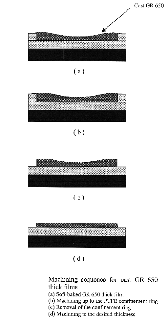
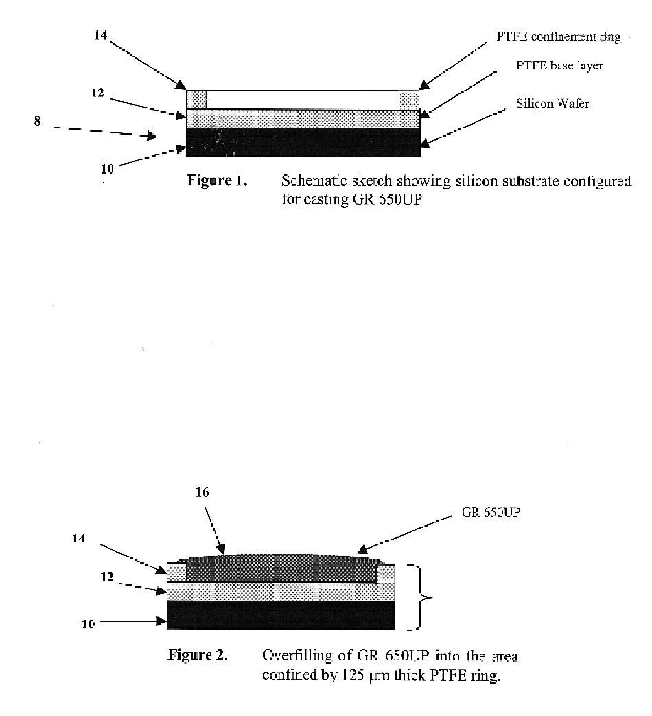
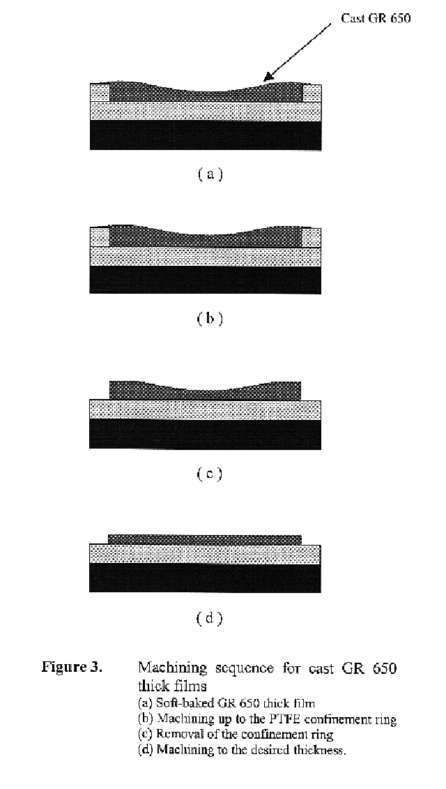
A 125 .mu.m thick DF1200 PTFE film was bonded onto a standard 4" silicon wafer (crystal orientation being of no consequence). A 540 um-thick silicon wafer provided sufficient rigidity for the purpose. Care was taken to prevent trapping air pockets while bonding the PTFE film. Excess film was trimmed off the edges of the wafer. This layer of PTFE was called the `base layer`. Another 125 .mu.m thick PTFE film was then cut in the shape of a ring and bonded on top of the first PTFE layer. This PTFE ring known as the `confinement ring` had an inner diameter of 82 mm. The outer diameter was not critical and could be any value that would accommodate the ring on the silicon wafer. The built-up configuration enabled casting of GR 650UP into it.

GR 650 casting and soft-baking were carried out using the Heraeus oven in the clean room at the Institute for Micromanufacturing (IfM) in Ruston, La. The followings are the steps involved in obtaining a thick GR 650 casting:

1. The substrate with the PT...

example 2

Another experiment similar to Example 1 was carried out to obtain a hardened SOG material with a 200 um thickness. The conditions were substantially the same as in Example 1, but the confinement ring was increased to at least 200 um. Sufficient SOG material was placed in the confined area to fill it to a depth of 200 um. The procedure in Example 1 was modified in that the bake temperature was 150.degree. C. rather than 75.degree. C. The bake time and ramp-up / ramp-down rates were the substantially the same as in Example 1.

While the foregoing describes the invention in terms of specific embodiment, those of skill in the art will see many modifications and variations which are within the scope of the present invention. Some such modifications and variations are attached in the thesis of Vijay-Anandh Shanmugam, which is attached as Appendix 1 and incorporated by reference. All such modifications and variation are intended to come within the scope of the following claims.

References

Marzol...


PUM


Abstract

A lithographic method for producing high aspect ratio silica micro-structures having the steps of: providing a carrier substrate with a confinement boundary placed on the carrier substrate; placing the SOG material within the confinement boundary and soft baking at a temperature above its glass transition temperature; forming a pattern of interest on the soft baked SOG material by x-ray lithography; and heating the SOG material until it is substantially converted to a silica-like oxide.

Description

BACKGROUND OF INVENTIONThe present invention relates to methods of producing optical micro-structures. In particular, the present invention relates to using x-ray lithography on thick films of SOG materials to form the micro-structures.There is an increasing use of integrated photonic and optoelectronic systems and a concurrent need for micro-optical components such as wave guides, couplers, lenses, prisms and similar devices for use in such systems. Silica is an excellent optical material because of its broad transmission range, low thermal expansion, high radiation hardness, mechanical strength and resistance to chemical attack. It is the basic constituent of optical fibers used in communication. Several prior art methods of producing silica micro-optical components begin with the step of forming silica films on a substrate such as a silicon wafer. These include a variety of chemical vapor deposition (CVD) and plasma-assisted deposition techniques. However, all these methods requi...

Claims


Application Information

Patent Timeline
IPC IPC(8): G02B6/13G02B6/132G02B6/136H01L21/02H01L21/316H01L21/311
CPCG02B6/132G02B6/136H01L21/31111H01L21/31608Y10S430/168H01L21/02318H01L21/02164
Inventor SHANMUGAM, VIJAY-ANANDHVASILE, MICHAEL J.COANE, PHILIP J.
Owner LOUISIANA TECH UNIV RES FOUND A DIV OF LOUISIANA TECH UNIV FOUND
Learn More