

High voltage integrated circuit amplifier
a high-voltage integrated circuit and amplifier technology, which is applied in the direction of dc-amplifiers with dc-coupled stages, amplifiers with semiconductor devices/discharge tubes, and low-frequency amplifiers. it can solve the problems of high-voltage transistors that are typically very large in comparison to low-voltage devices, gate of high-voltage mos transistors that cannot withstand more than approximately 30v with respect to the source, and reduce stress-effects. ,
- Summary
- Abstract
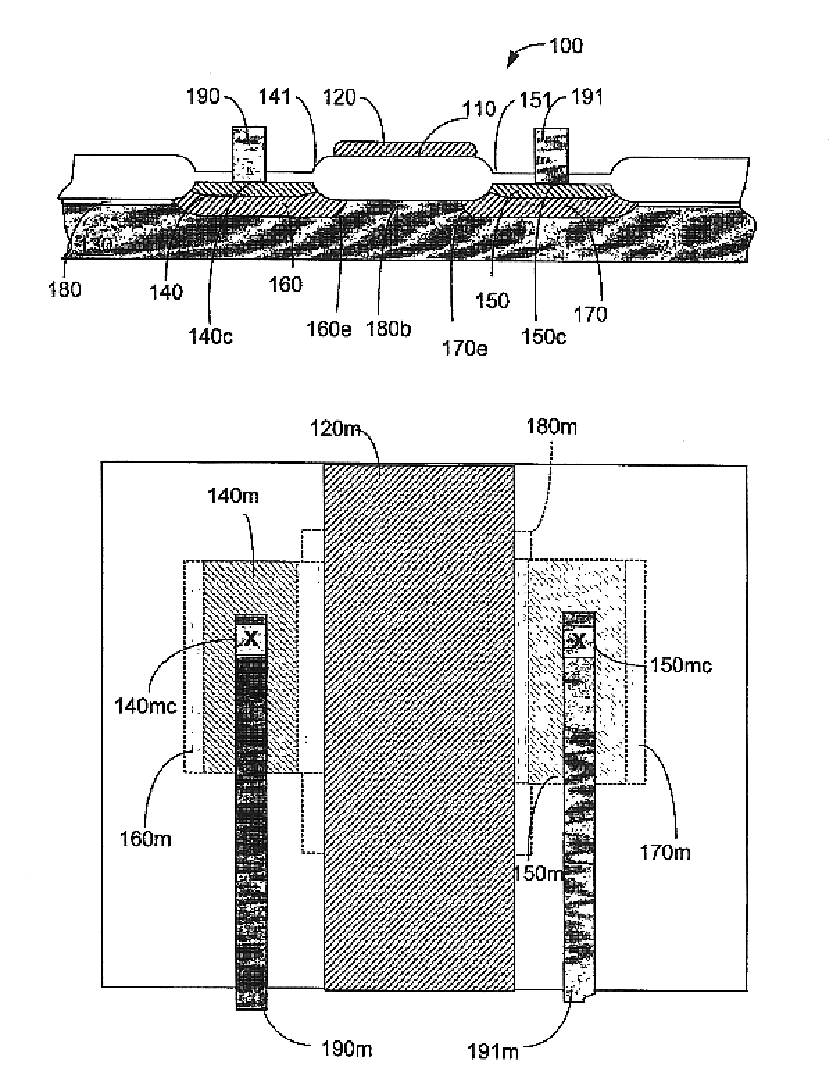
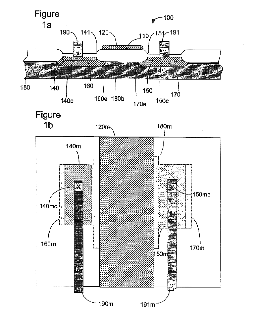
- Description
- Claims
- Application Information
AI Technical Summary
Benefits of technology
Problems solved by technology
Method used
Image

Examples
Embodiment Construction
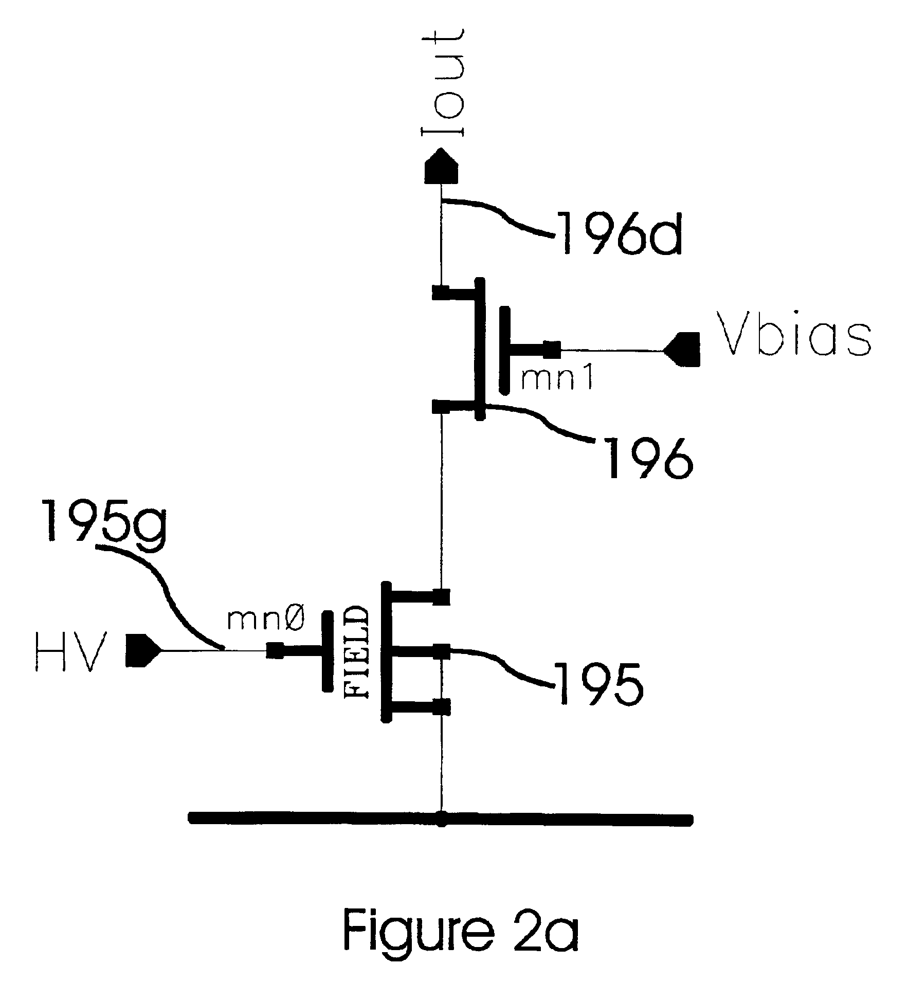
has been presented for purposes of illustration and description. It is not intended to be exhaustive or to limit the invention to the precise form disclosed. Many modifications and variations are possible in light of the above teaching. For example, a high-voltage amplifier with a gain may be attained using only one field transistor: e.g. a further embodiment of the invention includes replacing input transistor 212 with a low-voltage thin gate oxide transistor. The described embodiments were chosen in order to best explain the principles of the invention and its practical application to thereby enable others skilled in the art to best utilize the invention in various embodiments and with various modifications as are suited to the particular use contemplated. It is intended that the scope of the invention be defined by the claims appended hereto.
PUM
 Abstract
Description
Claims
Application Information