Nitride semiconductor device

a technology of semiconductor devices and nitride, which is applied in the direction of semiconductor devices, semiconductor lasers, lasers, etc., can solve the problems of high probability of device destruction, and achieve the effects of long life, high power output, and long li

Inactive Publication Date: 2005-01-04
NICHIA CORP
View PDF37 Cites 77 Cited by
  • Summary
  • Abstract
  • Description
  • Claims
  • Application Information

AI Technical Summary

Benefits of technology

[0014]Though, in a conventional multiple quantum well-type thereinafter referred to as MQW-type) nitride semiconductor device, all the barrier layers are, in general, doped with an n-type impurity, such as Si, in order to enhance light emission efficiency by increasing the initial electron concentration in the active layer, a nitride semiconductor device of the present invention has a barrier layer, that is doped with an n-type impurity in the same manner as in the prior art, while an n-type impurity is not substantially included only in the first barrier layer that is nearest to the p-type nitride semiconductor layer. In such a structure, characteristics with respect to the device lifetime and the reverse withstanding voltage of the nitride semiconductor device can be improved.
[0049](23) The above described p-type nitride semiconductor layer has a first p-type nitride semiconductor layer that contacts the above described active layer and becomes an electron confining layer and the active layer has a well layer of which the distance dB from the first p-type nitride semiconductor layer is in the range of from no less than 100 Å to no more than 400 Å and has a first barrier layer within the distance dB and, thereby, a nitride semiconductor device of which the device lifetime is excellent can be gained. This can be made to be a device structure wherein, as shown in FIG. 8, the distance dB from the first p-type nitride semiconductor layer 28 has a first barrier layer, that is to say, a barrier layer that does not substantially have an n-type impurity or that is adjusted to have a p-type impurity and, thereby, device deterioration due to the first p-type nitride semiconductor layer, which is a p-type carrier confining layer, is prevented so as to improve the device lifetime and it becomes possible to accelerate a light emitting recombination in a well layer arranged outside of the distance dB. Here, the device has, at least, the above described first barrier layer in the region of the distance dB, that is to say, the device has an impurity adjusted region, wherein, as described above, an impurity, or the amount of the impurity, is adjusted in at least a portion thereof in the region of the distance dB. At this time, the distance db is preferably the first barrier layer, that is to say, a first barrier layer of which the film thickness is dB is preferably formed so as to contact the first p-type nitride semiconductor layer so that the above described effects can be maximally gained. In this manner, by using the region of the distance dB as an impurity adjusted region, as shown in FIG. 8B, a structure can be gained wherein a plurality of layers of different band gap energies are provided. For example, in FIG. 8B a region 4, of which the band gap energy is smaller than that of the barrier layer 2c, is formed wherein the above described effects can be gained by making the region dB an impurity adjusted region. Contrarily, in a similar manner, a layer 4, which has band gap energy larger than that of the barrier layer 2b, may be provided. That is to say, in the case that a plurality of layers of which the band gap energies are different are provided in the region dB, a device of which the characteristics are excellent can be gained by adjusting the impurity, or the amount of the impurity, in the region dB which is used as the first barrier layer. Furthermore, the distance dB is preferably in the range of from no less than 120 Å to no more than 200 Å so that a nitride semiconductor device with an appropriate active layer in the device structure can be gained.

Problems solved by technology

Weak reverse withstanding voltage of the devices using nitride semiconductors has been a problem in the prior art, in that such devices have a high probability of destruction during handling in the manufacturing process and mounting on an end product.

Method used


Image

  • Nitride semiconductor device
  • Nitride semiconductor device
  • Nitride semiconductor device

Examples


example 1

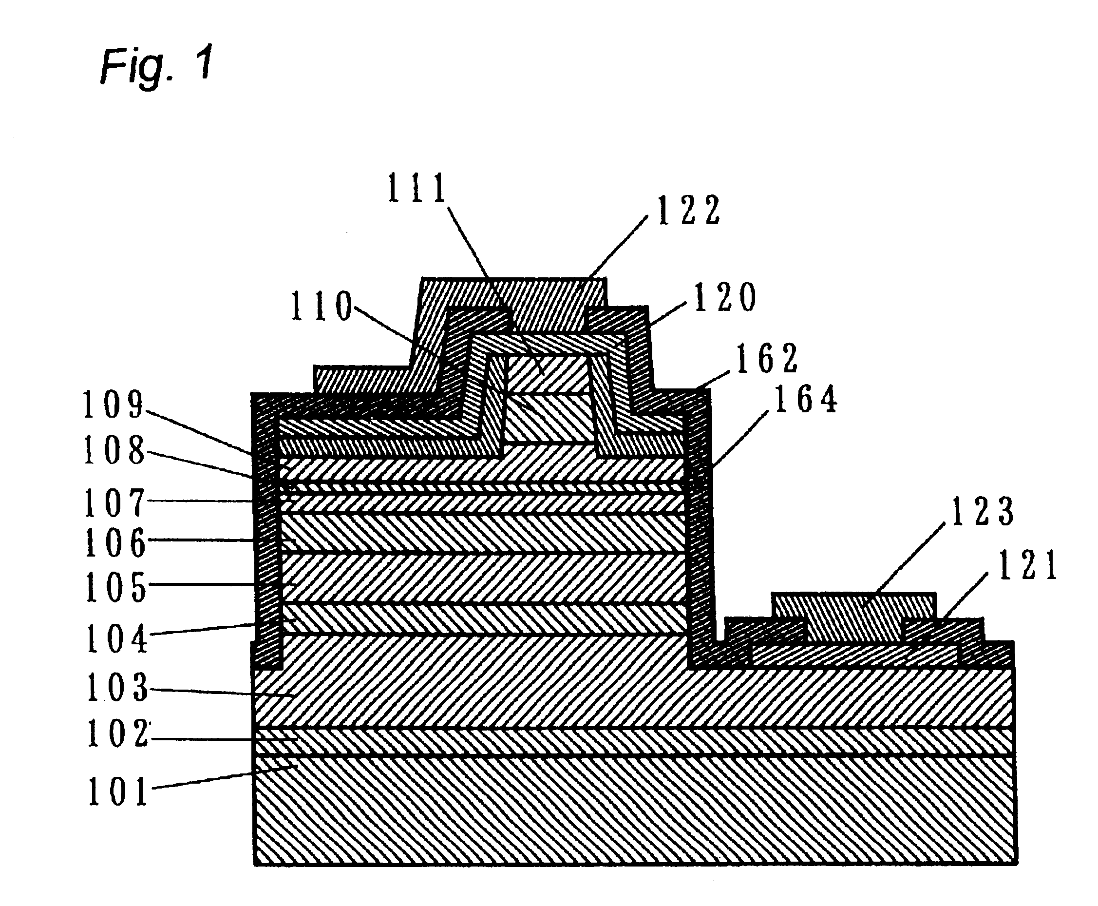
[0144]Now a laser device made of the nitride semiconductor device having the laser device structure as shown in FIG. 8 will be described below as an example.

[0145]While the substrate 101 is preferably made of GaN, a substrate of a material different from the nitride semiconductor may also be used. The substrate of different material may be made of an insulating substance such as sapphire or spinel (MgAl2O4) having principal plane in the C plane, R plane or A plane, or SiC (6H, 4H, 3C), ZnS, ZnO, GaAs, Si or a material other than nitride semiconductor which has been known to be capable of growing nitride semiconductor such as an oxide that undergoes lattice matching with the nitride semiconductor. Preferred material for making the substrate of different material is sapphire or spinel. The substrate of different material may be an off-angle one, in which case it has preferably stepwise off-angle construction for this allows base layer of gallium nitride to grow with good crystallinity...

example 2

[0181]Laser devices are made similarly to Example 1 except for the barrier layers located in the interface between the active layer and the p-type electron confinement layer (last-stacked barrier layer and barrier layer nearest to the p side), among the barrier layers provided in the active layer, are doped Mg in concentration of 1×10¹⁸ / cm3. The laser device thus obtained has the last barrier layer doped with Mg more heavily than in the case of Example 1, and has lifetime and reverse withstanding voltage characteristic of similar level.

example 3

[0182]Laser devices are made similarly to Example 1 except for the active layer is formed as described below.

[0183](Active Layer 107)

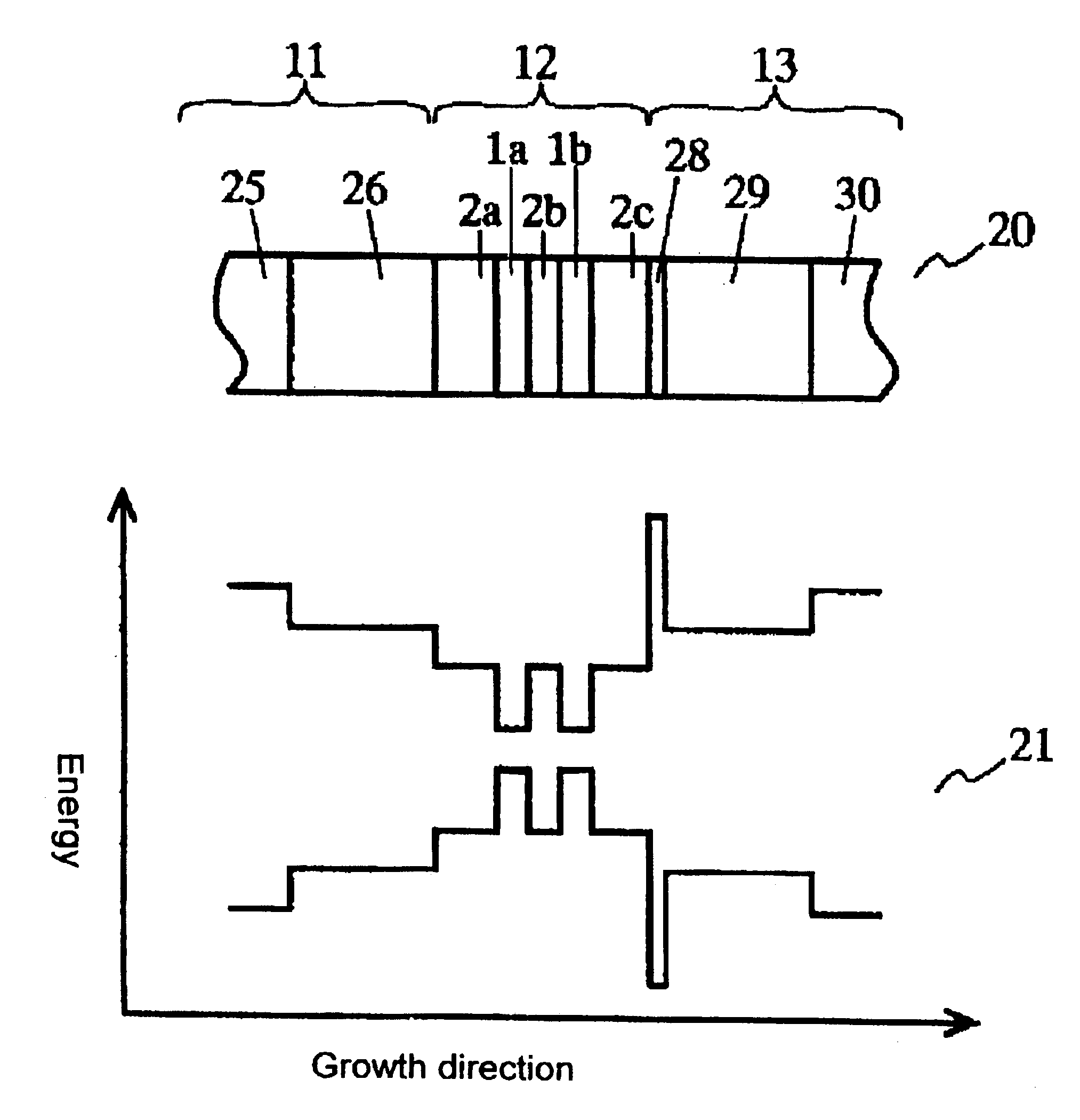
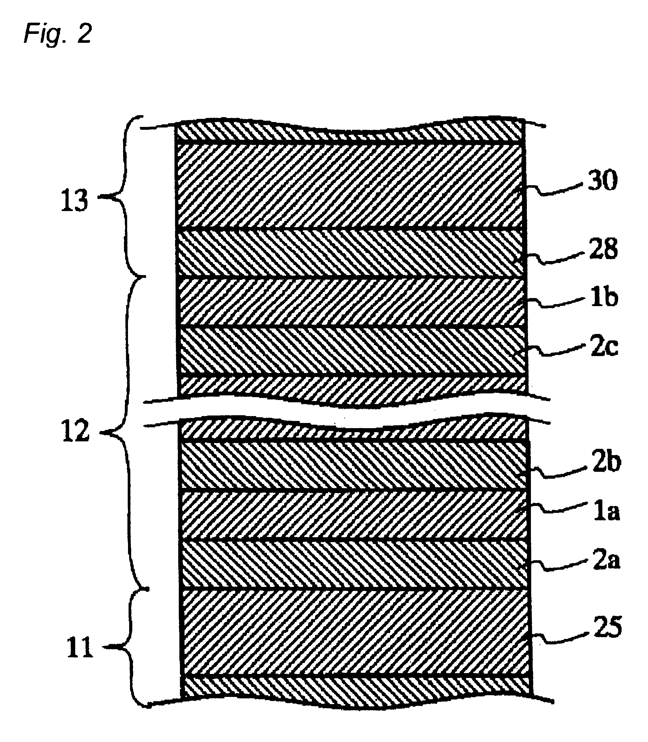
[0184]A barrier layer (B) made of In0.05Ga0.95N doped with Si in a concentration of 5×10¹⁸ / cm3 is formed to a thickness of 140 Å at a temperature of 800° C. by using TMI (trimethyl indium), TMG and ammonia as the stock material gas and silane gas as impurity gas. Then the supply of silane gas is stopped and a well layer (w) made of undoped In0.1Ga0.9N is formed to a thickness of 40 Å, while stacking the barrier layer (B) and the well layer (W) in the order of (B) / (W) / (B) / (W). Last, the last barrier layer made of undoped In0.05Ga0.95N is formed by using TMI (trimethyl indium), TMG and ammonia as the stock material gas. The active layer 107 becomes multiple quantum well structure (MQW) having total thickness of 500 Å.

[0185]A laser device capable of continuous oscillation at a wavelength of 405 nm with output power of 5 to 30 mW and threshold current dens...


PUM


Abstract

In the nitride semiconductor device of the present invention, an active layer 12 is sandwiched between a p-type nitride semiconductor layer 11 and an n-type nitride semiconductor layer 13. The active layer 12 has, at least, a barrier layer 2a having an n-type impurity; a well layer 1a made of a nitride semiconductor that includes In; and a barrier layer 2c that has a p-type impurity, or that has been grown without being doped. An appropriate injection of carriers into the active layer 12 becomes possible by arranging the barrier layer 2c nearest to the p-type layer side.

Description

[0002]This application is a divisional of application Ser. No. 09 / 898,460, filed Jul. 5, 2001, now U.S. Pat. No. 6,586,762, the entire content of which is hereby incorporated by reference in this application.BACKGROUND OF THE INVENTION[0003]1. Field of the Invention[0004]The present invention relates to a nitride semiconductor device which uses a nitride semiconductor (InXAlYGa1−X−YN, 0≦X, 0≦Y, X+Y≦1) used in light emitting devices such as light emitting diode device (LED) and laser diode device (LD), light receiving devices such as solar cell and optical sensor or electronic devices such as transistor and power devices, and particularly to a nitride semiconductor device comprising a nitride semiconductor layer which includes In.[0005]2. Description of the Prior Art[0006]Recently semiconductor laser devices which use nitride semiconductors have been receiving increasing demands for applications in optical disk systems such as DVD systems which are capable of recording and reproducin...

Claims


Application Information

Patent Timeline
Patent Type & Authority Patents(United States)
IPC IPC(8): H01S5/343H01L33/00H01S5/00H01S5/30H01S5/34H01S5/20H01L33/06H01L33/24H01L33/30H01L33/32
CPCB82Y20/00H01S5/343H01L33/32H01S5/34333H01L33/06H01L33/24H01S5/18308H01S5/18369H01S5/2009H01S5/22H01S5/305H01S5/3054H01S5/3086H01S5/3407H01S5/3415H01S2304/12
Inventor KOZAKI, TOKUYA
Owner NICHIA CORP
Why Eureka
Try Eureka