Preplating of semiconductor small outline no-lead leadframes

a semiconductor and leadframe technology, applied in the field of semiconductor devices and processes, can solve the problems of tolerance limits, serious jeopardizing good adhesion, and inability to fine-pitch devices to solder dipping, and achieve the effect of enhancing adhesion to molding compounds

Inactive Publication Date: 2005-01-04
TEXAS INSTR INC
View PDF8 Cites 13 Cited by
  • Summary
  • Abstract
  • Description
  • Claims
  • Application Information

AI Technical Summary

Benefits of technology

According to the present invention for a semiconductor integrated circuit (IC) leadframe, a continuous strip of sheet-like base metal is pre-plated with a layer of nickel fully covering the base metal, further on one surface with a palladium layer in a thickness suitable for bonding wire

Problems solved by technology

The harsh temperature variations involved in post-mold outer-lead plating of solder may seriously jeopardize good adhesion.
However, solder dipping is not practical for devices with fine-pitch leadframes because of solder bridging.
With small package geometries, there are tolerance limits with silver spot plating with negative effects on yield and cost.
One issue with this type of package is mold compound adhesio

Method used


Image

  • Preplating of semiconductor small outline no-lead leadframes
  • Preplating of semiconductor small outline no-lead leadframes
  • Preplating of semiconductor small outline no-lead leadframes

Examples


first embodiment

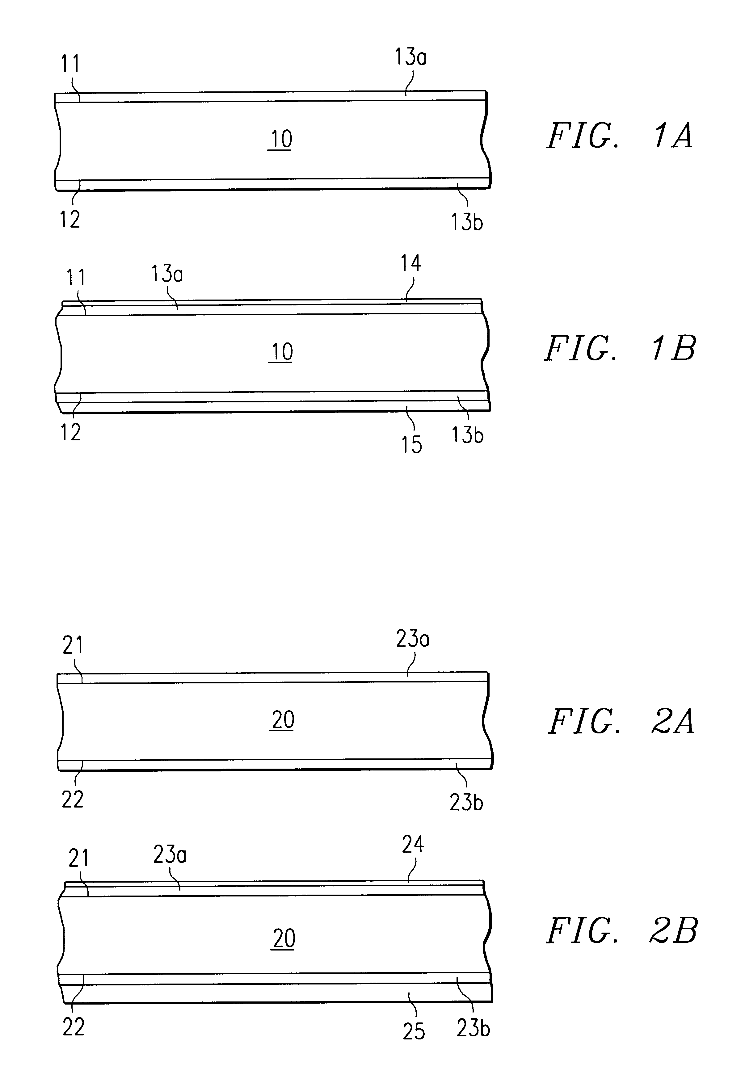
In the invention, depicted in FIGS. 1A and 1B, a layer of nickel is deposited onto both the first surface 11 of the base metal 10 (layer designated 13a in FIG. 1A) and the second opposite surface 12 (layer designated 13b in FIG. 1A). The nickel is flood plated so that both layers 13a and 13b have the same thickness in the range from about 0.5 to 3.0 μm.

Next, the nickel 13b covering the second surface 12 is protected by a simple mask covering the total surface of the sheet; then, a layer 14 of bondable metal is plated onto nickel layer 13a on the first surface 11 (see FIG. 1B). Palladium is the preferred choice for the bondable metal because of its added benefit of promoting good adhesion to molding compounds. Palladium layer 14 is thin and has only a thickness in the range from about 20 to 60 nm, but it ensures reliable bonding wire attachment (stitch bond, wedge bonds, and ball bonds). Need 1) of the above requirements is thus fulfilled.

Finally, the palladium layer 14 is protected ...

second embodiment

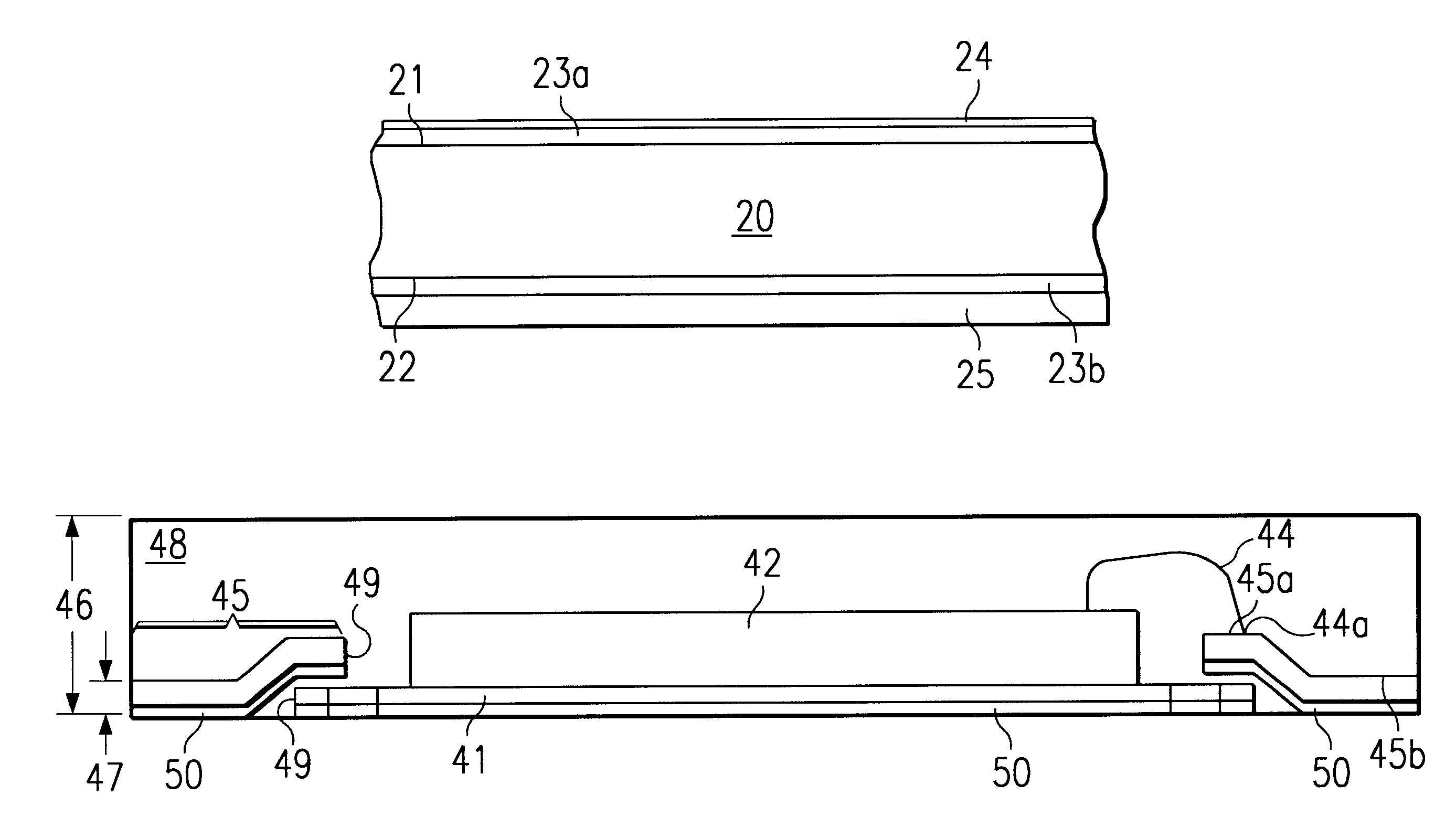
In the invention, depicted in FIGS. 2A and 2B, a continuous strip of sheet-like base metal 20, having first surface 21 and second opposite surface 22, is selected from a group consisting of copper, copper alloy, brass, aluminum, iron-nickel alloy, and invar. A layer of nickel is deposited onto both the first surface 21 of the base metal 20 (layer designated 23a in FIG. 2A) and the second opposite surface 22 (layer designated 23b in FIG. 2A). Layer thickness is in the range from about 0.5 to 3.0 μ.

Next, the nickel 23b covering the second surface 22 is protected by a simple mask; then, a layer 24 of bondable metal is plated onto nickel layer 23a on the first surface 21 (see FIG. 2B). Palladium in the range from about 20 to 60 nm thick is the preferred choice. It ensures reliable bonding wire attachment and good adhesion to molding compounds.

Finally, the palladium layer 24 is protected by a simple mask. A layer 25 of lead-free solder is plated onto nickel layer 23b on the second surfac...


PUM

PropertyMeasurementUnit
Fractionaaaaaaaaaa
Fractionaaaaaaaaaa
Thicknessaaaaaaaaaa

Abstract

For a leadframe for use with integrated circuit chips, a continuous strip of sheet-like base metal is pre-plated with a layer of nickel fully covering the base metal, further on one surface with a palladium layer in a thickness suitable for bonding wire attachment, and on the opposite surface with a layer of either palladium or lead-free solder in a thickness suitable for parts attachment. The leadframe structure is then stamped from the sheet so that the base metal is exposed at the stamped edges, enhancing adhesion to molding compounds.

Description

FIELD OF THE INVENTIONThe present invention is related in general to the field of semiconductor devices and processes and more specifically to the materials and preplating method of no-lead leadframes for integrated circuit devices.DESCRIPTION OF THE RELATED ARTThe leadframe for semiconductor devices was invented (U.S. Pat. Nos. 3,716,764 and 4,034,027) to serve several needs of semiconductor devices and their operation simultaneously: First of all, the leadframe provides a stable support pad for firmly positioning the semiconductor chip, usually an integrated circuit (IC) chip. Since the leadframe including the pads is made of electrically conductive material, the pad may be biased, when needed, to any electrical potential required by the network involving the semiconductor device, especially the ground potential.Secondly, the leadframe offers a plurality of conductive segments to bring various electrical conductors into close proximity of the chip. The remaining gap between the (“...

Claims


Application Information

Patent Timeline
IPC IPC(8): H01L23/495H01L23/31H01L23/28H01L23/48C23C28/02H01L23/50
CPCH01L23/3114H01L23/49551H01L23/49582H01L2924/15747H01L24/48H01L2924/14H01L2224/48091H01L2224/48247H01L2224/85464H01L2924/01046H01L2924/01078H01L2924/01079H01L2924/00014H01L2924/00H01L2224/451H01L2224/45124H01L2224/45144H01L2224/45147H01L2224/48864H01L2224/48664H01L2224/48764H01L24/45H01L2924/181H01L2224/05554H01L2224/48465H01L2924/00012
Inventor ABBOTT, DONALD C.MITCHELL, MICHAEL E.MOEHLE, PAUL R.
Owner TEXAS INSTR INC
Why Eureka
Try Eureka