Unique process chemistry for etching organic low-k materials

a low-k material, organic technology, applied in the direction of basic electric elements, semiconductor/solid-state device manufacturing, electric apparatus, etc., can solve the problems of poor profile control and yield reduction, slow operation of semiconductor devices, and the inability to effectively insulate the conductive lines of the dielectric layer formed of siosub>2 /sub>, so as to reduce the sputtering rate of inorganic hardmask material and the etching rate. , to achiev

Inactive Publication Date: 2005-01-11
LAM RES CORP
View PDF13 Cites 22 Cited by
  • Summary
  • Abstract
  • Description
  • Claims
  • Application Information

AI Technical Summary

Benefits of technology

The present invention teaches the addition of a fluorocarbon addition during etching to reduce both the sputtering rate of inorganic hardmask material and also the etch rate of the pho

Problems solved by technology

This introduces an increased level of coupling capacitance to the circuit, which has the drawback of slowing the operation of the semiconductor device.
As a consequence of the increasing line densities and operating frequencies in semiconductor devices, dielectric layers formed of SiO2 may not effectively

Method used


Image

  • Unique process chemistry for etching organic low-k materials
  • Unique process chemistry for etching organic low-k materials
  • Unique process chemistry for etching organic low-k materials

Examples


Embodiment Construction

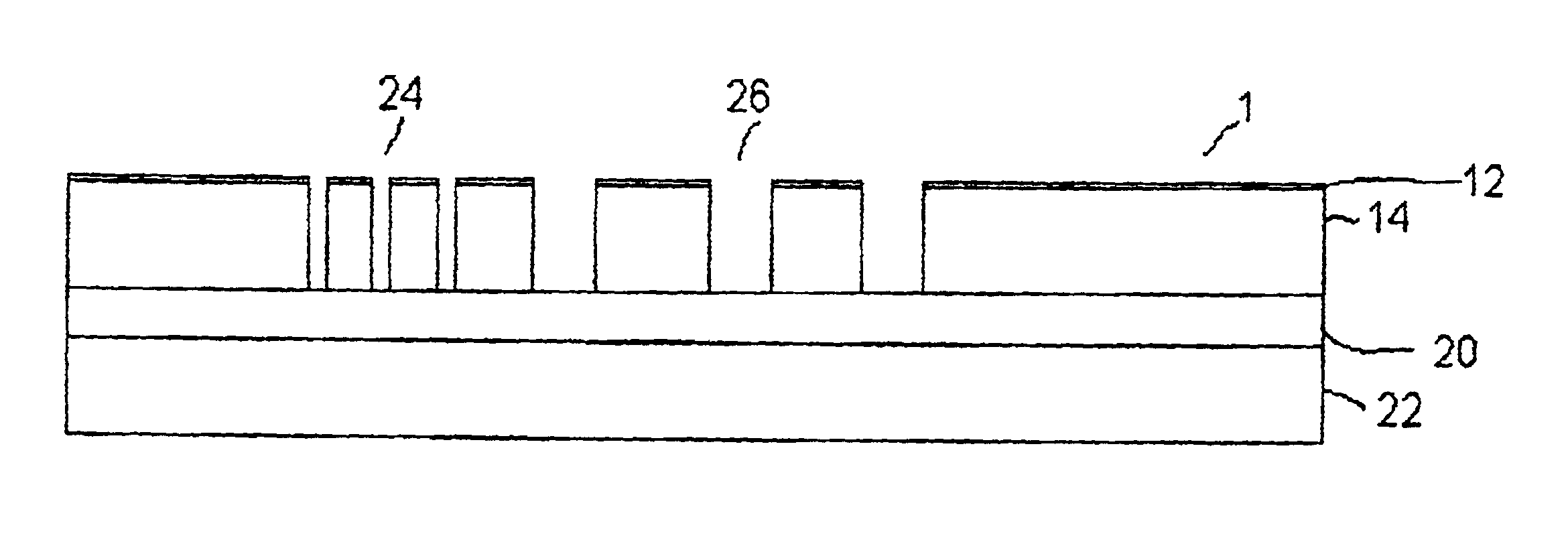
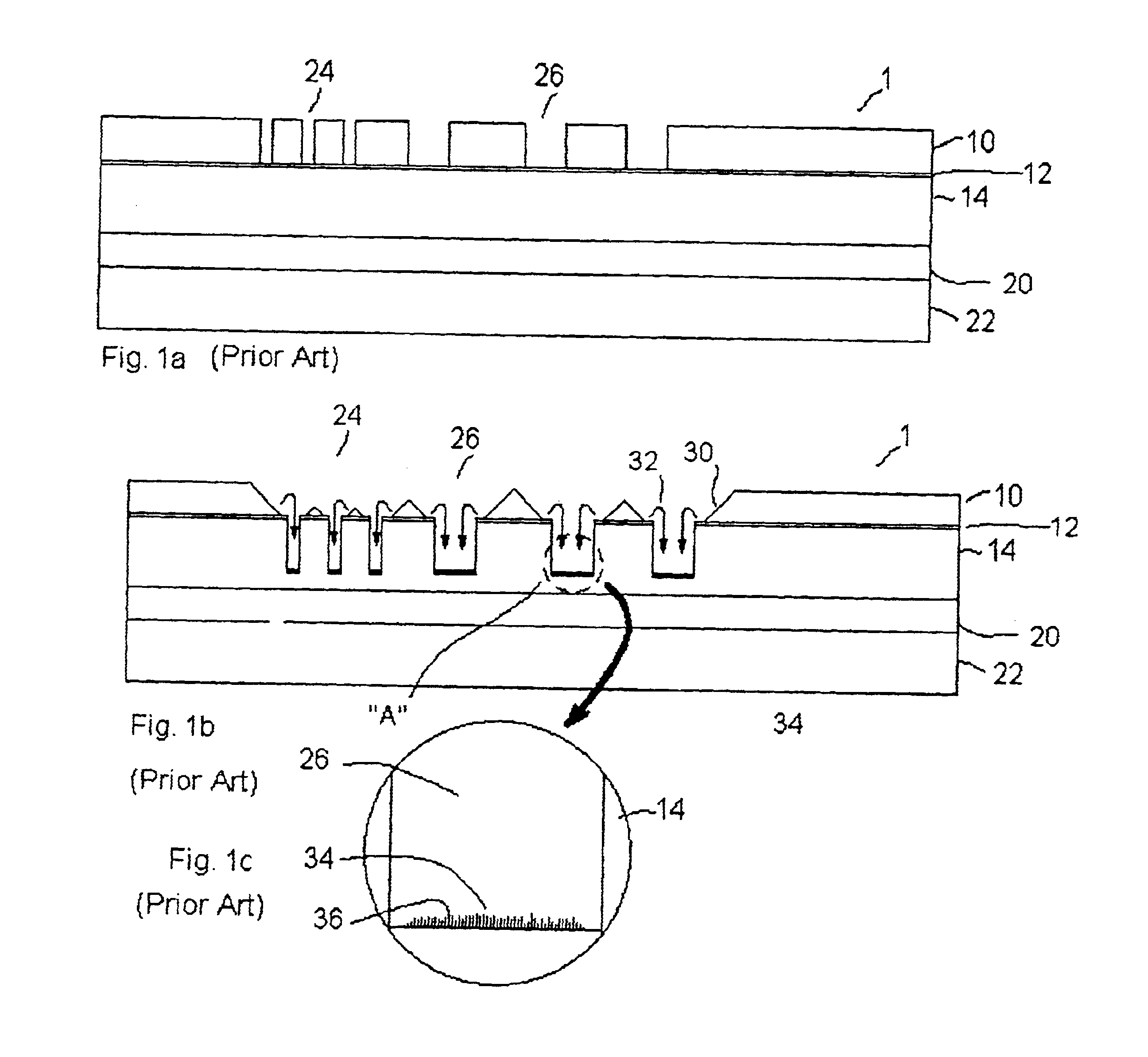
The present invention teaches a novel etch chemistry incorporating a fluorocarbon for etching a wide variety of feature sizes and shapes in wafers incorporating low-k dielectrics, especially dielectrics of an organic material, such as SiLK. The methodology taught herein eliminates the formation of micromasking from sputtered hardmask components during etching. The methodology taught herein further results in minimal RIE lag, minimal bowing of the vias and trenches formed by the etch process, good etch profiles, good resist selectivity, good etch rates, good CD control, and good etch uniformity across the wafer.

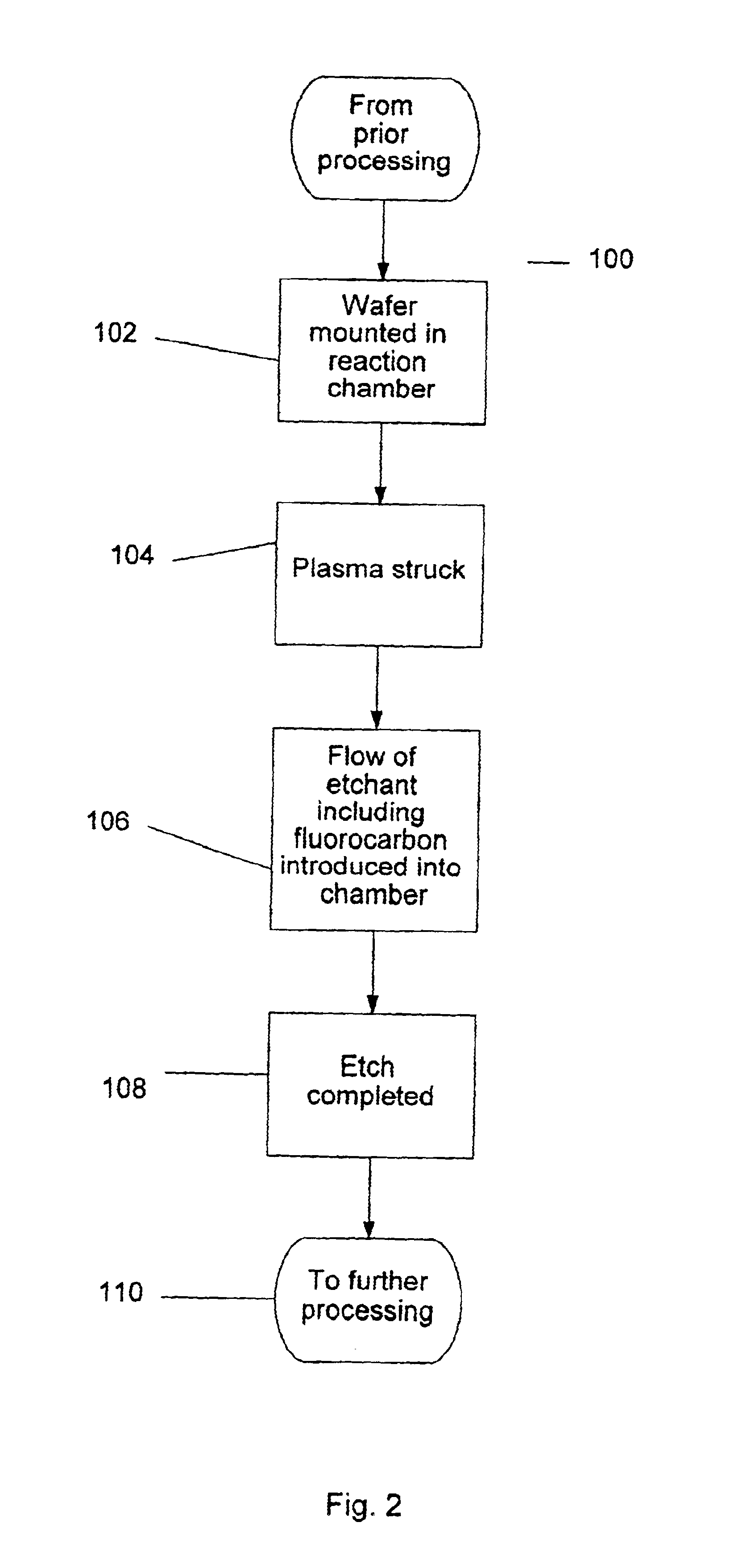
In order to etch a variety of features, including but specifically not limited to trenches and vias, in wafers including organic low-k dielectric, such as SiLK, layers the present invention implements the use of a fluorocarbon, for instance CH3F, methyl fluoride, as an adjunct during etching. The invention may provide a CH3F / H2 / N2 etchant gas, or a CH3F / NH3 etchant gas, or a C...


PUM


Abstract

Method for etching a feature in an integrated circuit wafer with minimized effect of micromasking. The method introduces a flow of etchant gas including a fluorocarbon gas to the wafer, and uses the etchant gas to form a plasma in proximity with at least a portion of the wafer. The plasma is used to etch at least a portion of the feature in the wafer. Disassociation of the fluorocarbon into fluorine and hydrocarbon species performs two functions. The fluorine species prevents or significantly reduces sputtered hardmask components from depositing on the floor of the etched feature during etching. The hydrocarbon species acts to form a passivation layer on the sidewalls of the feature.

Description

FIELD OF THE INVENTIONThe present invention relates to semiconductor manufacture. More particularly, the present invention relates to the etching of organic low-k dielectrics in semiconductor wafers.BACKGROUND OF THE INVENTIONIntegrated circuits use dielectric layers, which have typically been formed from silicon dioxide, SiO2, to insulate conductive lines on various layers of a semiconductor structure. As semiconductor circuits become faster and more compact, operating frequencies increase and the distances between the conductive lines within the semiconductor device decrease. This introduces an increased level of coupling capacitance to the circuit, which has the drawback of slowing the operation of the semiconductor device. Therefore, it has become important to use dielectric layers that are capable of effectively insulating conductive lines against such increasing coupling capacitance levels.In general, the coupling capacitance in an integrated circuit is directly proportional t...

Claims


Application Information

Patent Timeline
IPC IPC(8): H01L21/02H01L21/311
CPCH01L21/31138H01L21/3065
Inventor ZHU, HELEN H.BOWERS, JAMES R.MOREY, IAN J.BABIE, WAYNEGOSS, MICHAEL
Owner LAM RES CORP
Why Eureka
Try Eureka