Composite semiconductor wafer and a method for forming the composite semiconductor wafer

a composite semiconductor and semiconductor technology, applied in the direction of semiconductor/solid-state device details, coatings, microstructured devices, etc., can solve the problems of unsatisfactory bonding between the major surface of the wafer and the adjacent oxide layer or wafer, particle contamination of the wafer surface, manufacturing line, etc., to facilitate bonding

Inactive Publication Date: 2005-01-11
ANALOG DEVICES INC
View PDF4 Cites 43 Cited by
  • Summary
  • Abstract
  • Description
  • Claims
  • Application Information

AI Technical Summary

Benefits of technology

The advantages of the invention are many. The provision of the peripheral recess extending into the first major surface of the first wafer around the periphery thereof, either removes surface imperfections around the periphery of the first major surface if such surface imperfections were present on the first major surface of the first wafer, and / or provides clearance for any surface imperfections in the corresponding peripheral area of the first major surface of the second wafer. Accordingly, with the surface imperfections removed around the periphery of the first major surface of the first wafer and clearance being provided for surface imperfections around the first major surface of the second wafer, the composite wafer can be formed with the first and second wafers without leaving an unbonded portion extending around the periphery of the composite wafer. Thus, where the first major surfaces of the first and second wafers are to be bonded directly to each other, the remaining portion of the first major surface of the first wafer defined by the peripheral recess is bonded directly to the corresponding area of the first major surface of the second wafer, and the two first major surfaces are bonded together over their entire area without any unbonded peripheral portions, provided of course no other surface imperfections are present on the first major surfaces of the first and second wafers. On the other hand, where a buried layer is to be located between the first major surfaces of the first and second wafers, the buried layer may be formed on one or both of the first major surfaces. In either case, the absence of surface imperfections on the first major surface of the first wafer and / or the provision of clearance for the surface imperfections on the first major surface of the second wafer, resulting from the peripheral recess, facilitates bonding of the first major surface of the one of the first and second wafers to the buried oxide layer, or bonding of the two oxide layers over the entire interface surfaces without any unbonded peripheral areas. The formation of the peripheral recess removes the peripheral portion of the first wafer which would otherwise have remained unbonded to the second wafer, or where the buried layer or a portion thereof is formed on the first major surface of the first wafer, the portion of the buried layer which would otherwise have remained unbonded to the second wafer or a buried layer thereon does not exist, due to the presence of the peripheral recess in the first wafer.
Another advantage of the invention is that once the first and second wafers have been bonded either directly together or with a buried layer therebetween, as the case may be, to form the composite wafer, no further etching, grinding or otherwise treating or machining the first wafer to remove an unbonded peripheral portion is required as is the case in prior art methods. Thus, there is no danger of damage to the first or second wafers or to the buried layer, which would otherwise arise using prior art methods in the removal of the unbonded peripheral portion, since the composite wafer is formed by the method according to the invention without any unbonded peripheral portions.
By forming the peripheral recess to a depth from the first major surface of the first wafer, which is at least equal to the thickness to which the first wafer is to be finished after the composite wafer is formed, the peripheral recess defines the periphery of the first wafer when the thickness of the first wafer has been reduced to its finished thickness, and no further etching or machining of the first wafer is required in order to define its periphery. Additionally, when the peripheral recess is formed to a depth equal to or just greater than the finished thickness to which the first wafer is to be finished, the etch time for etching the peripheral recess is optimised where the peripheral recess is formed by etching, and the machining time is optimised where the peripheral recess is to be formed by machining.
A particularly important advantage of the invention is that the method according to the invention is suitable for use with composite wafers having device and handle wafers forming device and handle layers of any desired thicknesses and ratio of thickness. There is no limit to the thickness ratio of the handle layer to the device layer, nor is there any limit of the ratio of the thickness of the handle wafer and the device wafer to the thickness of material ground from the device wafer, as is the case where the peripheral edge of the device wafer is subsequently ground after bonding of the device and handle wafers together in order to remove the unbonded peripheral portion of the device wafer. Since the peripheral imperfections are removed from the device wafer, and / or clearance is provided for peripheral imperfections on the handle wafer, prior to bonding of the device and handle wafers together, the ratio of the thickness of the handle wafer to the device wafer is irrelevant, as is the ratio of the thickness of the handle and device wafers to the thickness of material ground from the device wafer. However, it is desirable that the peripheral recess should be formed to a depth at least equal to and preferably greater than the final finished thickness of the device layer, so that when the device lay is ground to its final finished thickness, the peripheral surface defined by the peripheral recess forms the peripheral edge of the device layer. This, thus, avoids any need for subsequent removal of the peripheral edge of the first wafer which would otherwise overhang the peripheral recess.

Problems solved by technology

This peripheral ridge on the major surface of the device layer forming wafer, which when the composite wafer is formed faces the handle layer, in general, inhibits satisfactory bonding of the wafers around the peripheral edges thereof.
This problem arises irrespective of whether a buried oxide layer or other buried layer is located between the two wafers or not.
However, an annular band extends around the major surfaces of the wafers towards the peripheral edge thereof where bonding between the major surface of the wafer and the adjacent oxide layer or wafer is unsatisfactory.
If the unbonded peripheral portion is left an the composite wafer, when the device layer forming wafer is machined to the appropriate thickness to form the device layer, the unbonded peripheral portion of the device layer tends to shatter and break off during transportation or subsequent processing, thus causing particle contamination of the wafer surface, the manufacturing line and other problems.
Additionally, shattering of the device layer forming wafer adjacent the unbonded peripheral portion may also occur during mechanical polishing of the device layer forming wafer after the device layer forming wafer has been machined to the desired final thickness.
Shattering of the unbonded peripheral portion of the device layer forming wafer during polishing leads to scratching of the polishing surface, which is undesirable.
In general, these methods for removing the unbonded periphery of the device layer forming wafer are unsatisfactory, and suffer from a number of problems.
Firstly, the grinding method whereby the unbonded periphery of the device layer forming wafer is ground from the composite wafer, depending on the grinding machine used, is often only suitable for semiconductor wafers where the total thickness of the handle and the device layer forming wafers prior to grinding to the thickness of the amount of material removed during grinding is more than two to one.
This, thus, prevents the use of this method for composite wafers having a relatively thick device layer and a relatively thin handle layer combination, in other words, a relatively thick silicon on oxide layer SOI and a handle layer which is relatively thin.
Additionally, in this grinding method a subsequent chemical etch is required in order to remove crystal damage caused to the surface of the handle layer forming wafer around the peripheral edge of the composite wafer by the grinding, and the chemical etch attacks both the buried oxide layer and the back surface of the handle layer forming wafer, which is undesirable.
The masking methods require relatively expensive equipment for patterning the exposed major surface of the device layer forming wafer.
The step is formed in the handle layer due to the fact that the edge area of the composite wafer adjacent the bond interface is uneven, and cannot be masked, thereby leaving the edge area exposed to the etchant, which etches the step in the handle layer.
The use of a dry etch with the masking method is unsuitable for relatively deep device layer forming wafers, due to attack by the etching gas on the underside and edges on the handle layer forming wafer.

Method used


Image

  • Composite semiconductor wafer and a method for forming the composite semiconductor wafer
  • Composite semiconductor wafer and a method for forming the composite semiconductor wafer
  • Composite semiconductor wafer and a method for forming the composite semiconductor wafer

Examples


Embodiment Construction

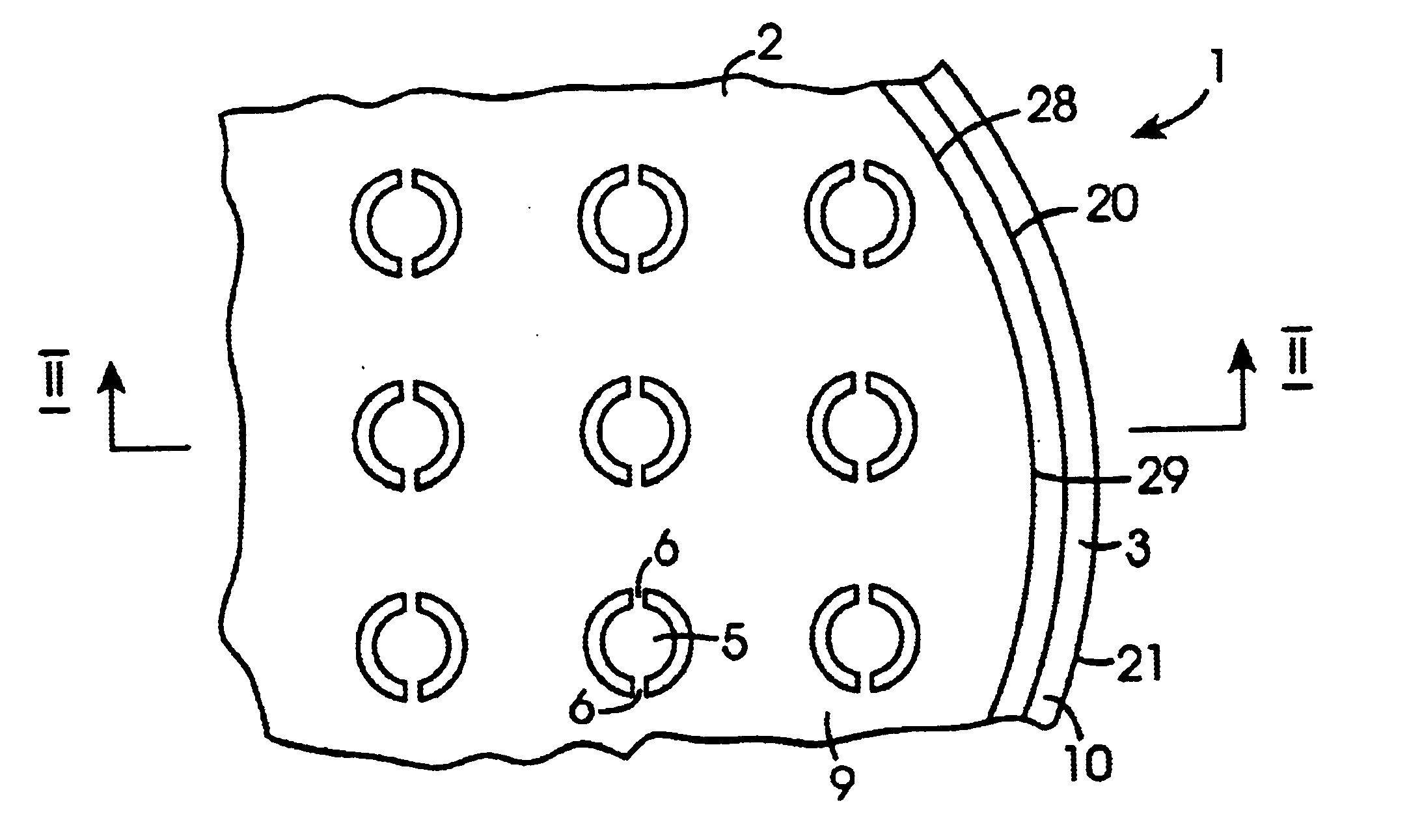
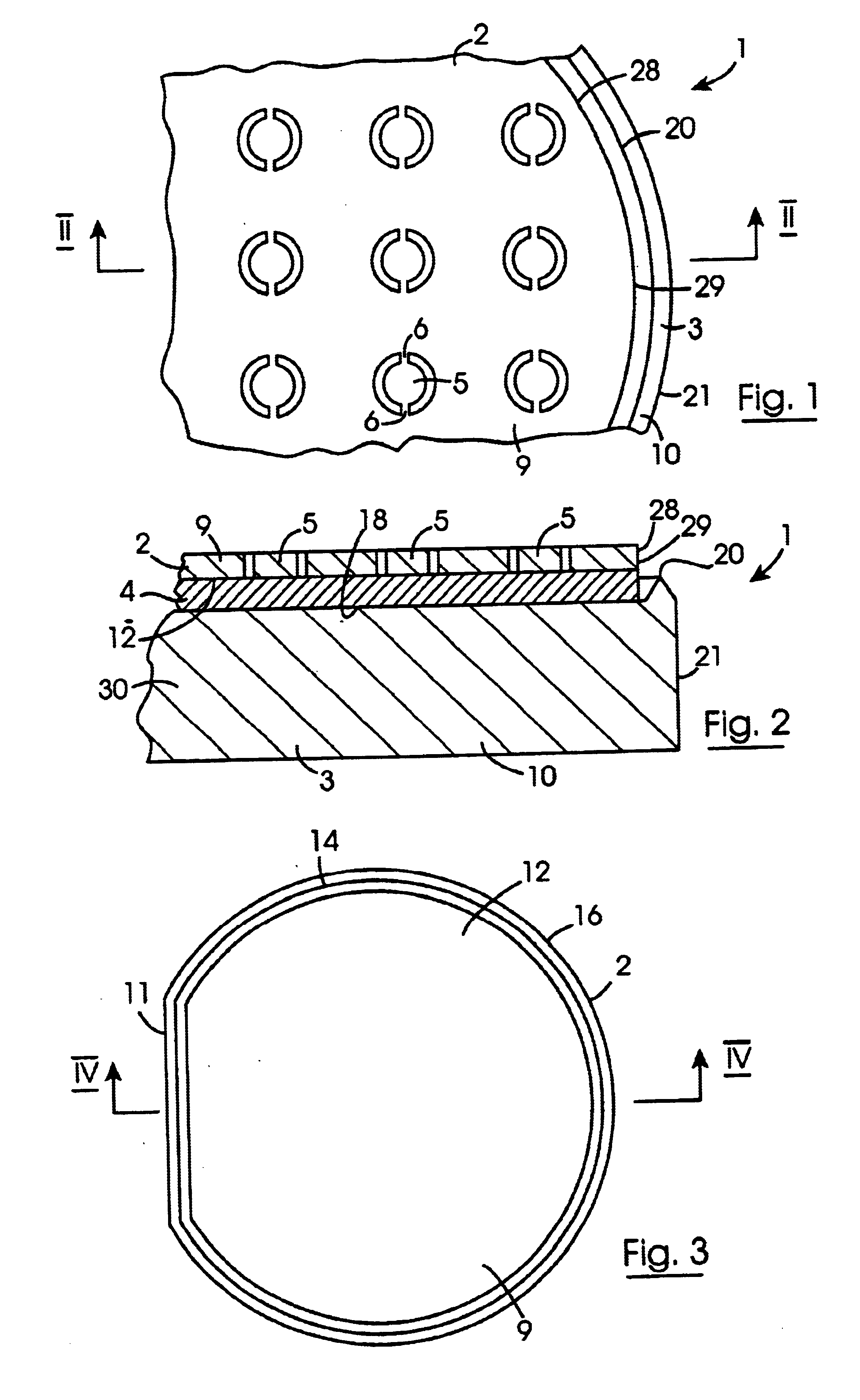
Referring to the drawings, which are not to scale, and initially to FIGS. 1 and 2, there is illustrated a composite semiconductor wafer according to the invention, indicated generally by the reference numeral 1. formed by a method according to the invention. The composite wafer 1 is an SOI (silicon on insulator) and comprises a device layer 2 supported on a handle layer 3 with a buried oxide layer 4 located between the device and handle layer 2 and 3, respectively. A plurality of micro-mechanical components, in this embodiment of the invention micro-mirrors 5 are formed in the device layer 2 and are tiltably connected to the device layer 2 by tethers 6. Bores (not shown) would typically be etched through the handle layer 3 and the buried oxide layer 4 for accommodating electrodes to the micro-mirrors 5 for tilting thereof. The arrangement and formation of such bores and micro-mirrors in a device layer of a composite wafer will be well known to those skilled in the art.

Referring now ...


PUM

PropertyMeasurementUnit
thicknessaaaaaaaaaa
thicknessaaaaaaaaaa
thicknessaaaaaaaaaa

Abstract

A composite SOI semiconductor wafer (1) comprises a device layer (2) and a handle layer (3) with a buried oxide layer (4) located between the device and handle layers (2,3). The device and handle layers (2,3) are formed from device and handle wafers (9,10), respectively. A peripheral ridge (14) extending around a first major surface (12) of the device wafer (9) adjacent the peripheral edge (16) thereof is removed by etching a peripheral recess (25) to a depth (d) into the device wafer (9) prior to bonding the device and handle wafers (9,10), in order to avoid an unbonded peripheral pardon extending around the composite wafer (1). The depth to which the peripheral recess (25) is etched is greater then the final finished thickness t of the device layer (2). An oxide layer (22) is grown on the device water (9) and a photoresist layer (23) on the oxide layer (22) is patterned to define the peripheral recess (25). The oxide layer (22) is etched leaving only a portion of the oxide layer (22) beneath the photoresist layer (23), which subsequently forms the oxide layer (4). The peripheral recess (25) is then etched, and the photoresist layer (23) is removed. The oxide layer (22) is fusion bonded to a first major surface (18) of the handle wafer (10) by a high temperature bond anneal. Thereafter the device layer (2) is machined to its final finished thickness t.

Description

FIELD OF THE INVENTIONThe present invention relates to a method for forming a composite semiconductor wafer, and the invention also relates to a composite semiconductor wafer formed by the method.BACKGROUND TO THE INVENTIONIn the fabrication of micro-mechanical components and electronic semiconductor devices in semiconductor wafers, a composite semiconductor wafer is formed. The composite wafer comprises a device layer in which the micro-mechanical components and / or the electronic semiconductor devices are to be formed and which is provided by a device layer forming wafer of semiconductor material, typically, silicon. The device layer is supported on a handle layer, which is formed by a separate handle layer forming wafer, also of semiconductor material, and typically, silicon. In general, the handle layer is a relatively thick layer formed from a wafer of thickness of 350 μm or greater, while the device layer is a relatively thin layer, and may be of thickness as thin as 1 μm, and ...

Claims


Application Information

Patent Timeline
Patent Type & Authority Patents(United States)
IPC IPC(8): H01L21/762H01L21/70B81C1/00
CPCB81C1/00357H01L21/76251B81C2201/019
Inventor MACNAMARA, CORMAC JOHNNEVIN, WILLIAM ANDREWPETERS, GRAEME
Owner ANALOG DEVICES INC
Why Eureka
Try Eureka