Inspection and repair of active type substrate

a liquid crystal device and active type technology, applied in the direction of liquid/fluent solid measurement, surface reaction electrolytic coating, electrochemical machining apparatus, etc., can solve the problems of performance index, channel etch type has a production capacity problem, display image persistence, etc., to achieve easy restoration to its sound condition, increase the insulating characteristics of the polyimide layer 71, and delay the appearance of abnormalities in displayed images

Inactive Publication Date: 2005-01-18
PANASONIC CORP
View PDF22 Cites 3 Cited by
  • Summary
  • Abstract
  • Description
  • Claims
  • Application Information

AI Technical Summary

Benefits of technology

The invention is associated with a technique of filling a pinhole with an organic insulating material. Even though a pinhole is filled with an organic insulating material, there is no problem as far as insulating characteristics necessary for devices can be attained. In view of this fact, a solution containing about 0.01% polyamic acid salt is selected as an electrodeposition solution from materials that enable formation by electrodeposition, as described in “T IEE Japan” (Vol. 112, No. 12, 1992) and a plus potential is applied to the scan lines 11 while a minus potential being applied to the electrode plate 61, whereby the pinhole 44 can be filled up with a polyimide layer 71 as shown in FIG. 15(2). With an electrodeposition voltage of about 10V, the thickness of the polyimide layer 71 can be easily made to be 1 μm. After precipitation of the polyimide layer 71, it is preferable to increase the insulating characteristics of the polyimide layer 71 by applying heat treatment at 200 to 300° C. for several to several tens of minutes. Heating conditions may be experimentally determined as they are dependent on the heat resistance of the insulated gate transistors and the composition of the material of the liquid crystal. The repairing method of this embodiment has the advantage that any materials can be used for the scan lines (and the opposed electrodes and / or the common capacitance lines).
The seventh embodiment relates to a technique of discontinuing the scan line in a pinhole area. In cases where a scan line material such as Cr, Mo and Ti that enables electrolytic treatment by a chemical solution is used in contrast with the foregoing two embodiments, the electrochemical treatment system of the invention is used; an electrolytic solution such as nitric acid or hydrochloric acid about 0.1 N is used as the chemical solution 62; and a plus potential is applied to the scan lines 11 while a minus potential being applied to the electrode plate 61 composed of a SUS plate, whereby a scan line in the pinhole 44 is dissolved into the electrolytic solution 62 in the form of positive Cr, Mo and Ti ions, so that Cr, Mo and Ti thin films are precipitated on the surface of the electrode plate 61. The electrolytic treatment is continued for an appropriate period of time, namely, several minutes to ten-odd minutes to dissolve the scan line 11 within the pinhole 44 by about several μm, thereby forming a chipped portion 71 as shown in FIG. 16. Although it depends on the pattern width of the scan line 11, the scan line 11 in the region where a pinhole is present may be removed in the form of the pinhole for line discontinuation. In this case, as far as a redundancy arrangement or remedy circuit is provided, the active substrate can be easily restored to its sound condition.
Usually, 10 to 50 V is enough for bath voltage. By virtue of the elimination of the scan line 11 within the pinhole 44, even if the liquid crystal penetrating through the pinhole electrically reacts with the remaining scan lines 11, it takes a time for the ions generated by the electrochemical reaction to pass through the narrow space having a height of 0.3 μm (which corresponds to the thickness of the scan line 11) at the highest. As a result, appearance of abnormalities in displayed images can be delayed. This leads to improved reliability.

Problems solved by technology

Secondly, since the quality of the passivation insulating layer is usually extremely poor, such an unfavorable situation must be avoided that electric charges are accumulated within the passivation insulating layer resulting in the persistence of displayed images.
Regarding the operation of the PCVD system and particle generation, the channel etch type has a problem in production capability.
In addition, it has a problem in performance index since the mobility of electrons is small.
As understood from the foregoing description, the fabrication of active type liquid crystal image displays is quite complicated and requires high precision.
Therefore, defects inevitably occur in various modes.
As a result, defect modes such as checked and dealt with in the various inspections are rarely found by the end users or consumers and rarely cause damage nor troubles to them.
However, some defect modes occur after long-run jobs or long use, although it is always the case with other products.
This aging inspection is not so expensive when conducted on a certain production lot, but incurs tremendous cost when all products are tested for more than several hours.
Occurrence of such a pinhole is often caused by inclusion of minute foreign matters or particles during the formation of the insulating layer used for fabricating the active substrate 2 and impossible to be prevented with the current technology.
It is also difficult to prevent occurrence of pinholes in a photosensitive resin during the photolithography process which is repeated several times. Dust generated particularly in the gate insulating layer is unavoidable because of the characteristics of the PCVD system, so that pinholes are likely to occur in the gate insulating layer.
However, the ordinary passivation insulating layer made of SiNx is poor in coverage because it is formed at low temperature as described earlier.
This is the cause of the above-described defect mode.
In short, if a pinhole having a size of 1 lm or less is present in the gate insulating layer, the pinhole is not filled up with the passivation insulating layer so that it is impossible to prevent occurrence of defects.
Therefore, when an aging inspection is made to check such a liquid crystal, there is imposed a serious burden.
The aging inspection takes a long time particularly in the case of IPS mode liquid crystal panels because the opposed electrodes of the IPS mode have a smaller area, compared to those of TN mode liquid crystal panels so that current does not flow smoothly.
Even when a pinhole inspection is done with the most up-to-date automatic optical inspection system in the fabrication process in order to solve the above problem, the currently available resolving power is insufficient (the resolution prescribed by the specification is 1.5 μm).
It can be easily imagined that even if a high resolving power optical inspection system was available, it would take more than several minutes to inspect one active substrate, and as a result, the inspection cost would be forced to increase tremendously.
However, this leads to an increase in the cost of the passivation insulating layer formation process.
Another conceivable attempt is such that the formation temperature of the passivation insulating layer is raised to about 300° C. to improve the coverage of the passivation insulating layer, but this also reveals a drawback.
Concretely, where the semiconductor layer is a-Si, it has low heat resistance so that the mobility μ of electrons becomes lower, causing degradation of the electric characteristics of the insulated gate transistor.
In consequence, difficulties arise in the application of lug the insulated gate transistor to large-screen or high precision liquid crystal panels.
Therefore, a significant number of steps are needed for delivery and installation in a plant and in addition, this requires a clean room with a high ceiling, accompanied with the increased capacity of the clean room and therefore increased air conditioning cost.
Also, treatment systems, which deal with chemical solutions, have a cost problem in the maintenance of the clean room, because there is a high possibility of generation of a large amount of chemical mist so that a large amount of air needs to be exhausted for the sake of security and hygiene.
As has been described above, it is difficult to cover the conductive pattern on the substrate with an insulating layer free from pinholes and such pinholes are likely to be the main cause of various defects particularly in the substrate of display devices.

Method used


Image

  • Inspection and repair of active type substrate
  • Inspection and repair of active type substrate
  • Inspection and repair of active type substrate

Examples


first embodiment

(First Embodiment)

A first embodiment of the invention will be described with particular reference to FIG. 11. In FIG. 11, parts and elements corresponding to those of the prior art explained earlier are indicated with the same reference numerals as in the prior art and there is omitted an explanation on them. This is equally applied to other figures and embodiments.

An active substrate 2 is conveyed from the outside of an in-substrate selective electrochemical treatment system or from a substrate storage container within the treatment system by a conveyor means (not shown) such as a robot arm to be installed and horizontally retained on a stage 60. There is a mechanism for holding the substrate 2 by use of vacuum suction. Then, an electrode plate 61 is made to be close to the active substrate 2 and an electrolytic solution 62 such as nitric acid adjusted for example 01 N (normal) is dropped onto a gap between the active substrate 2 and the electrode plate 61. For this purpose, an app...

second embodiment

(Second Embodiment)

A second embodiment is designed such that a sponge impregnated with a chemical solution is adhered to the inner surface of the electrode plate.

In this embodiment, as shown in FIG. 12, a sponge 620 impregnated with a chemical solution is adhered to the inner surface of the electrode plate 61 opposed to the active substrate 2. The chemical solution is confined in a specified region by pressing the electrode plate 61 against the active substrate 2. After completion of the pin hole inspection, the electrode plate 61 is moved away from the active substrate 2 and the chemical solution adhered to the active substrate 2 is recovered and removed. Then, the active substrate 2 is separated from the stage, and taken out of the chemical treatment system after the chemical solution is further removed. It is apparent that the material of the sponge and the material of the member for adhering or fixing the sponge to the electrode plate 61 must be selected taking chemical resistan...

third embodiment

(Third Embodiment)

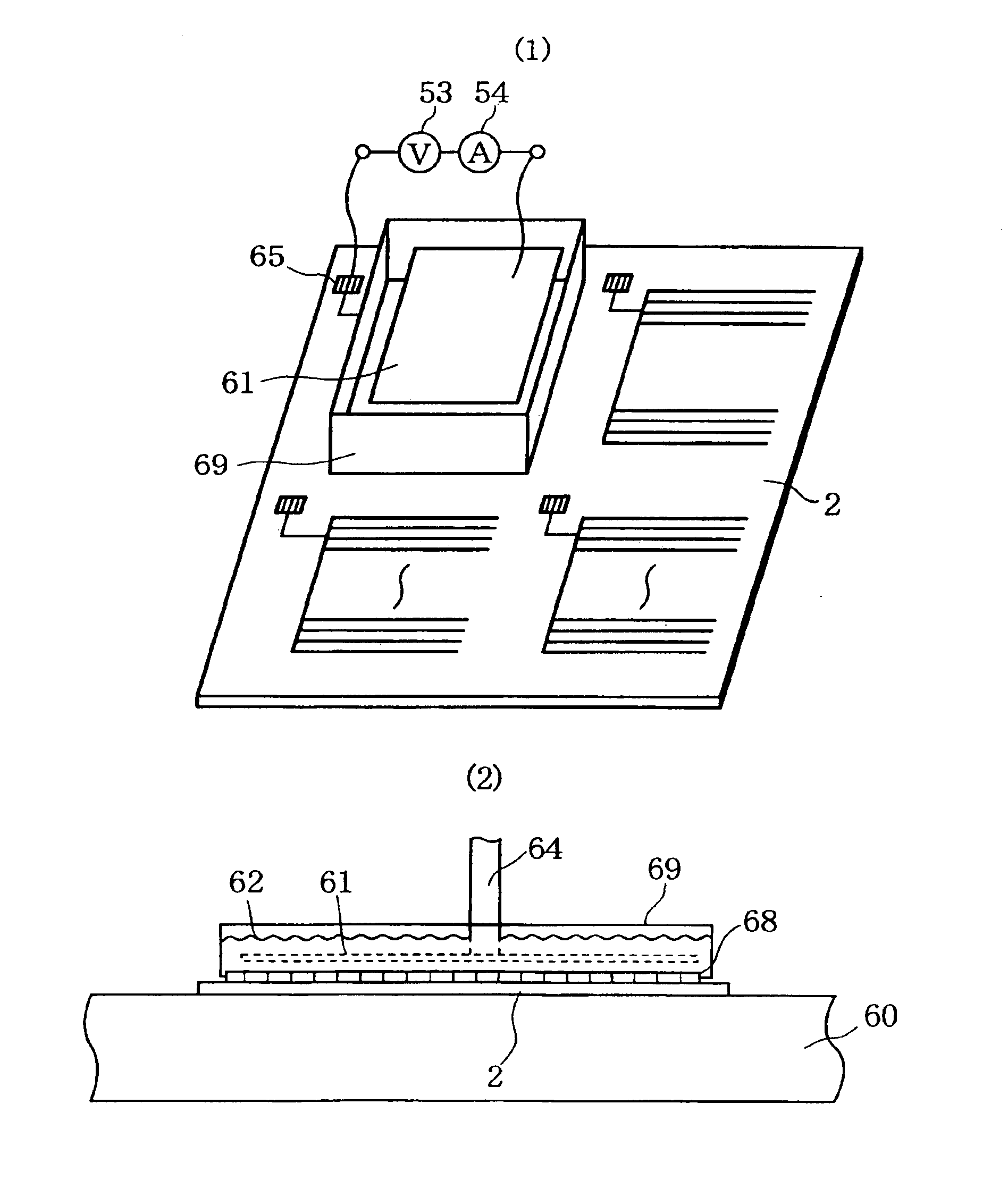
A third embodiment uses a frame-shaped container.

Reference is made to FIG. 13 for describing the third embodiment of the invention.

First, the active substrate 2 is placed on the stage 60 to be held horizontally there on. Then, a frame-shaped container 69 is pressed against the active substrate 2, the frame-shaped container 69 having an opening slightly larger than the electrode plate 61 at its upper and lower ends and a sealing material 68 embedded at its lower end. Then, the electrode plate 61 is inserted into the frame-shaped container 69 and held in a stationary condition at a position several mm or more apart from the active substrate 2. Subsequently, an appropriate electrolytic solution 62 such as nitric acid 0.1 N is dropped into the frame-shaped container 69. Note that reference numeral 64 designates a supporting bar for holding, lifting and lowering the electrode plate 61. A mechanism for holding, lifting and lowering the frame-shaped container 69 is simple...


PUM

PropertyMeasurementUnit
lengthaaaaaaaaaa
thicknessaaaaaaaaaa
thicknessaaaaaaaaaa

Abstract

An in-substrate selective electrochemical treatment system for finding and repairing pinholes of an active substrate including holding an insulating substrate having a conductive pattern, supplying a predetermined amount of a specified chemical solution to a specified region on the insulating substrate and confining it in the specified region, locating the reversed polarity electrode plate close to the insulating substrate such that the reversed polarity electrode plate comes in contact with the chemical solution on the upper surface of the insulating substrate, bringing the electrode into contact with the conductive pattern in the periphery of the insulating substrate, applying a specified direct current between the electrode and the reversed polarity electrode plate, and measuring a value of current flowing between the electrode and the reversed polarity electrode plate.

Description

TECHNICAL FIELDThe present invention relates to devices using a liquid crystal and particularly to techniques for aging tests, pinhole inspection and repair of active type liquid crystal devices.BACKGROUND ART(General Background Art)Thanks to recent developments in miniaturization, liquid in crystal materials, high density packaging techniques and others, various types of image display devices (e.g., televisions that employ a liquid crystal panel having a diagonal line length of 5 to 50 cm) are Ad presently manufactured and marketed on a large scale. Further, color displaying is easily enabled by forming red, green and blue colored layers on either one of two glass substrates that constitute a liquid crystal panel. This tendency is noticeable particularly in the so-called active type liquid crystal panels having a switching element for every pixel, because they have less crosstalk and capability of displaying high contrast images at high response speed.While the matrix structures of...

Claims


Application Information

Patent Timeline
Patent Type & Authority Patents(United States)
IPC IPC(8): G02F1/13G09G3/00C25D11/00C25F3/14G02F1/136G02F1/1368G09F9/00G09F9/30H01L29/786
CPCG09G3/006G02F1/1309G02F1/1362G02F2203/69H01L21/306
Inventor KAWASAKI, KIYOHIRO
Owner PANASONIC CORP
Why Eureka
Try Eureka