Integrated circuit comprising an auxiliary component, for example a passive component or a microelectromechanical system, placed above an electronic chip, and the corresponding fabrication process

a technology of integrated circuits and components, applied in the direction of instruments, soldering devices, photomechanical devices, etc., can solve the problems of discrete nature of solder bumps that do not protect the side walls of components, damage to the interconnects nor the components to be covered by the chip procedure, and no method of protecting both components, so as to optimize the mechanical integrity of the whole assembly and improve the mechanical strength of the assembly

Inactive Publication Date: 2005-01-25
STMICROELECTRONICS SRL
View PDF6 Cites 26 Cited by
  • Summary
  • Abstract
  • Description
  • Claims
  • Application Information

AI Technical Summary

Benefits of technology

In other words, according to the invention, the chip on a standard semiconductor wafer and the auxiliary component on another specific wafer are produced independently. Thus, there is no risk of the processes involving the auxiliary component damaging the chip interconnects.
Moreover, the use of a virgin wafer as support for producing the auxiliary component greatly widens the choice of material processes, independently of the constraints associated with the interconnects.
The use of a buried layer (intermediate layer) allows fine control of the thickness of the layer which will cover the electronic chip, that is to say the thickness of the second substrate. Etching of the vias (interconnect holes) is thereby considerably facilitated and the thickness of the whole assembly remains compatible with the standard packaging processes. In addition, this process permits, as final passivation, a wide choice of materials compatible with the radiofrequency performance required, should this be necessary.
Moreover it is particularly advantageous that the production of each second contact pad comprises the formation of an orifice passing through the pad. Thus, after a second pad has been brought into contact with a corresponding first pad, a rivet is made by metallization in the orifice of the second pad. In other words, metallization of the vias which pass through the protective cover electrically connect the two wafers and improve the mechanical strength of the assembly by generating microscopic rivets. The latter may be distributed where the designer chooses, at key points on the chip so as to optimize the mechanical integrity of the whole assembly.
Although various options are provided for carrying out the step of mutual adhesion of the two substrates, such as for example the use of a polymer material, it is particularly advantageous for this adhesion to be carried out by low-temperature molecular bonding. This prevents any circuit from being damaged. Moreover, molecular bonding preserves the option of carrying out both the electrical connection and the mechanical connection, whereas if an adhesion technique using a polymer material between the contact pads is employed, it is necessary to provide an electrical connection at a point other than at the contact pads.

Problems solved by technology

This flip-chip procedure damages neither the interconnects nor the component to be covered.
However, the discrete nature of the solder bumps does not protect the side walls of the component, for example a microswitch.
Thus, in the prior art, no method allows both the component to be protected and the electrical contacting, indispensable for packaging, to be guaranteed.
Added to this limitation are further drawbacks which are associated with the contemplated approach and which complicate the integration.
To avoid any damage to the lower interconnect levels, this production must not involve temperatures above 450° C. However, this constraint in particular prevents the use of specific materials, such as certain dielectrics having a very high permittivity.
Moreover, the processes of the prior art finally end up with a stack substantially greater than 500 microns in height, which no longer allows the standard packaging procedures to be applied.
It is then necessary to thin the cover, but its handling then becomes a tricky operation because of its mechanical fragility.
Moreover, once the wafers have been assembled, it becomes difficult to perform further technological operations because of the non-uniformity of the thickness of the adhesive polymer and of the solder bumps which mean that the upper surface has a poor flatness.

Method used


Image

  • Integrated circuit comprising an auxiliary component, for example a passive component or a microelectromechanical system, placed above an electronic chip, and the corresponding fabrication process
  • Integrated circuit comprising an auxiliary component, for example a passive component or a microelectromechanical system, placed above an electronic chip, and the corresponding fabrication process
  • Integrated circuit comprising an auxiliary component, for example a passive component or a microelectromechanical system, placed above an electronic chip, and the corresponding fabrication process

Examples


Embodiment Construction

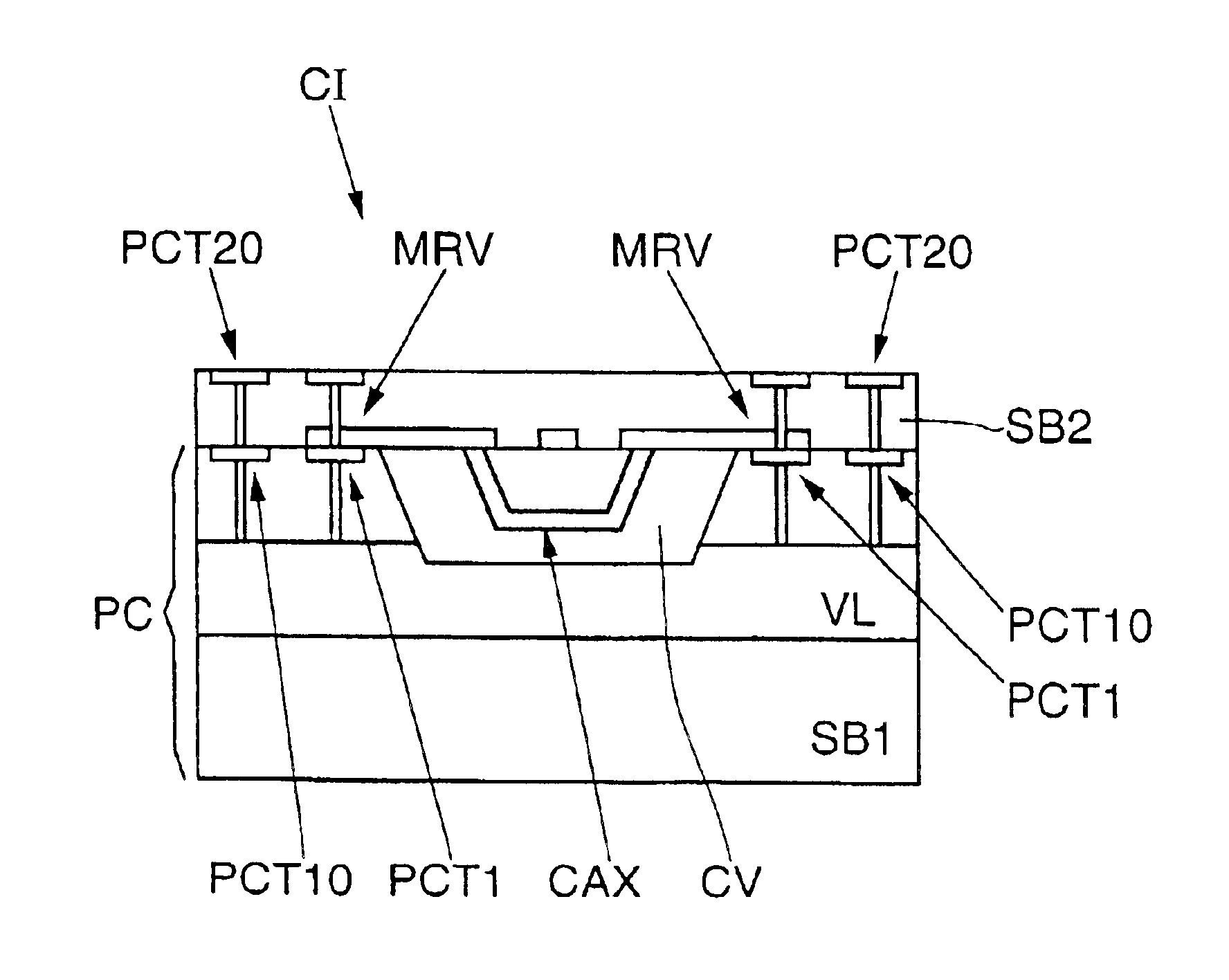
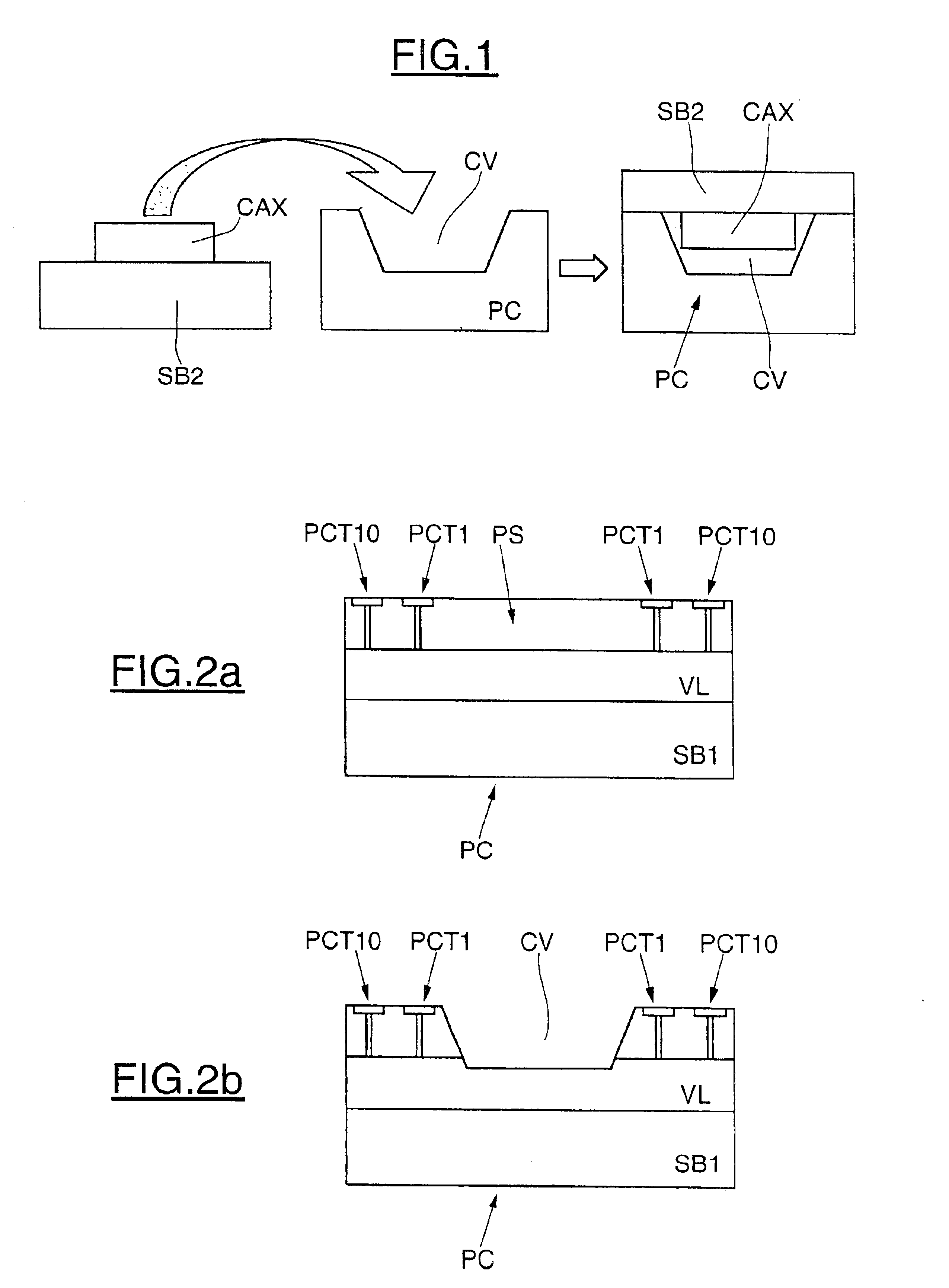
In the left-hand part of FIG. 1, the reference SB2 denotes a semiconductor substrate on which an auxiliary component CAX, for example a passive component, or else a microelectromechanical system, has been produced.

Moreover, on a substrate separate from the substrate SB2, in a conventional manner known per se, an electronic chip PC is produced and a cavity CV intended to house the component CAX is provided, at a chosen point, in the upper portion of this electronic chip PC.

Next, as illustrated in the right-hand part of FIG. 1, the upper face (which has become the lower face in the right-hand part of FIG. 1) of the substrate SB2 is fastened to that part of the upper face of the electronic chip lying outside the cavity CV.

An integrated circuit is then obtained which, after packaging, comprises an assembly consisting of an electronic chip PC and an auxiliary component CAX, the upper surface of which assembly is approximately plane.

This method of implementing the invention will now be ex...


PUM

PropertyMeasurementUnit
temperaturesaaaaaaaaaa
heightaaaaaaaaaa
adhesionaaaaaaaaaa

Abstract

The fabrication of an integrated circuit includes a first phase of producing an electronic chip and a second phase of producing at least one auxiliary component placed above the chip and of producing a protective cover which covers the auxiliary component. The first phase of producing the chip is effected from a first semiconductor substrate and comprises the formation of a cavity lying in a chosen region of the chip and emerging at the upper surface of the chip. The second production phase includes the production of the auxiliary component from a second semiconductor substrate, separate from the first, and then the placement in the cavity of the auxiliary component supported by the second substrate and the mutual adhesion of the second substrate to the upper surface of the chip lying outside the cavity. The second substrate then also forms the protective cover.

Description

CROSS-REFERENCE TO RELATED APPLICATIONThis application is based upon and claims priority from prior French Patent Application No. 01 15594, filed on Dec. 3, 2001, the entire disclosure of which is herein incorporated by reference.BACKGROUND OF THE INVENTION1. Field of the InventionThe invention relates to integrated circuits and more particularly to the incorporation of auxiliary components, such as high-performance passive components or microelectromechanical systems, on an electronic chip.2. Description of the Related ArtThe development of microelectronic technologies has been accompanied by an increasingly systematic integration of complex electrical functions, hitherto located outside the package of the integrated circuit. Among these functions, mention may be made of microelectromechanical systems (MEMS) and passive components known to those skilled in the art as above-IC components produced above the passivation layer covering the integrated circuit.The production of these MEM...

Claims


Application Information

Patent Timeline
Patent Type & Authority Patents(United States)
IPC IPC(8): B81B7/00B81C3/00
CPCB81C1/0023B29C2043/5825
Inventor FARCY, ALEXISCORONEL, PHILIPPEANCEY, PASCALTORRES, JOAQUIN
Owner STMICROELECTRONICS SRL
Why Eureka
Try Eureka