Semiconductor device including voltage conversion circuit having temperature dependency

a technology of voltage conversion circuit and temperature dependency, which is applied in the direction of logic circuit coupling/interface arrangement, pulse technique, instruments, etc., can solve the problems of disadvantageous irregular temperature dependency of voltage conversion circuit and significant problem of increase of standby current due to a refresh operation, etc., to achieve greater temperature characteristics and eliminate irregularities

Inactive Publication Date: 2005-02-01
RENESAS ELECTRONICS CORP
View PDF1 Cites 46 Cited by
  • Summary
  • Abstract
  • Description
  • Claims
  • Application Information

AI Technical Summary

Benefits of technology

According to another invention, the voltage conversion circuits equal in the connection relationship of circuit elements are cascaded to each other to form voltage conversion circuit stages, and each stage includes a resistance section having a positi

Problems solved by technology

For the portable device driven by a battery, however, the increase of standby current due to a refresh operation which is essential to the DRAM cell is considerably problematic.
However, it is known that the temperature dependency of the voltage

Method used


Image

  • Semiconductor device including voltage conversion circuit having temperature dependency
  • Semiconductor device including voltage conversion circuit having temperature dependency
  • Semiconductor device including voltage conversion circuit having temperature dependency

Examples


first embodiment

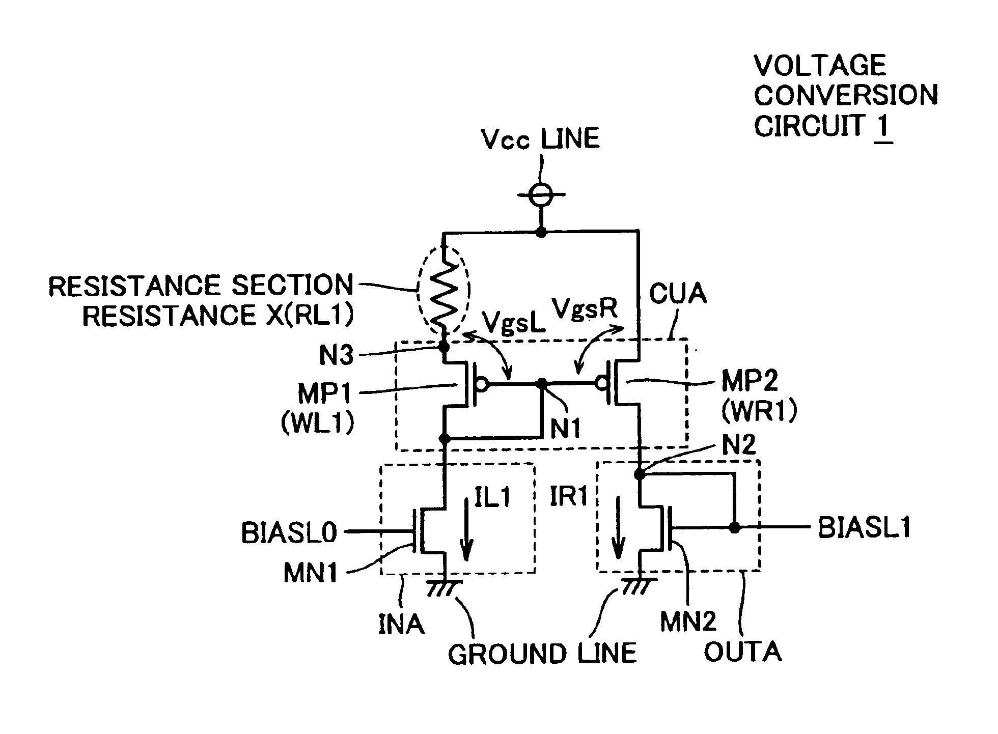
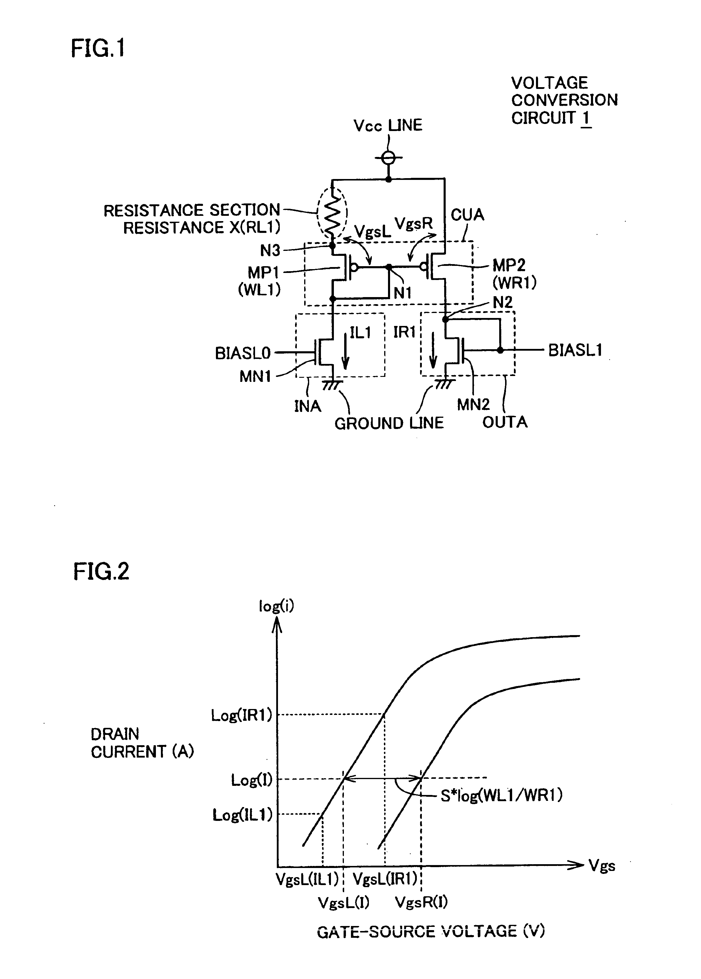
In FIG. 1, a voltage conversion circuit according to a first embodiment is formed of an input section INA which is connected to a ground line serving as the first voltage line and to which an input voltage BIASL0 of voltage conversion circuit 1 is inputted, an output section OUTA which is connected to a ground line and which outputs an output voltage BIASL1 of voltage conversion circuit 1 according to input voltage BIASL0, a current-mirror section CUA which is connected to a Vcc line serving as the second voltage line and which changes an output current IR1 carried to output section OUTA according to an input current IL1 that is carried to input section INA according to input voltage BIASL0, and a resistance section which is connected between the Vcc line and current-mirror section CUA.

It is noted that output current IR1 and output voltage BIASL1 change as the resistance value of the resistance section changes according to temperature change.

In addition, when the changes of input an...

second embodiment

In the second embodiment, a case where voltage conversion circuit 1 in the first embodiment is applied to a ring oscillator for the refresh timer of DRAM will be described.

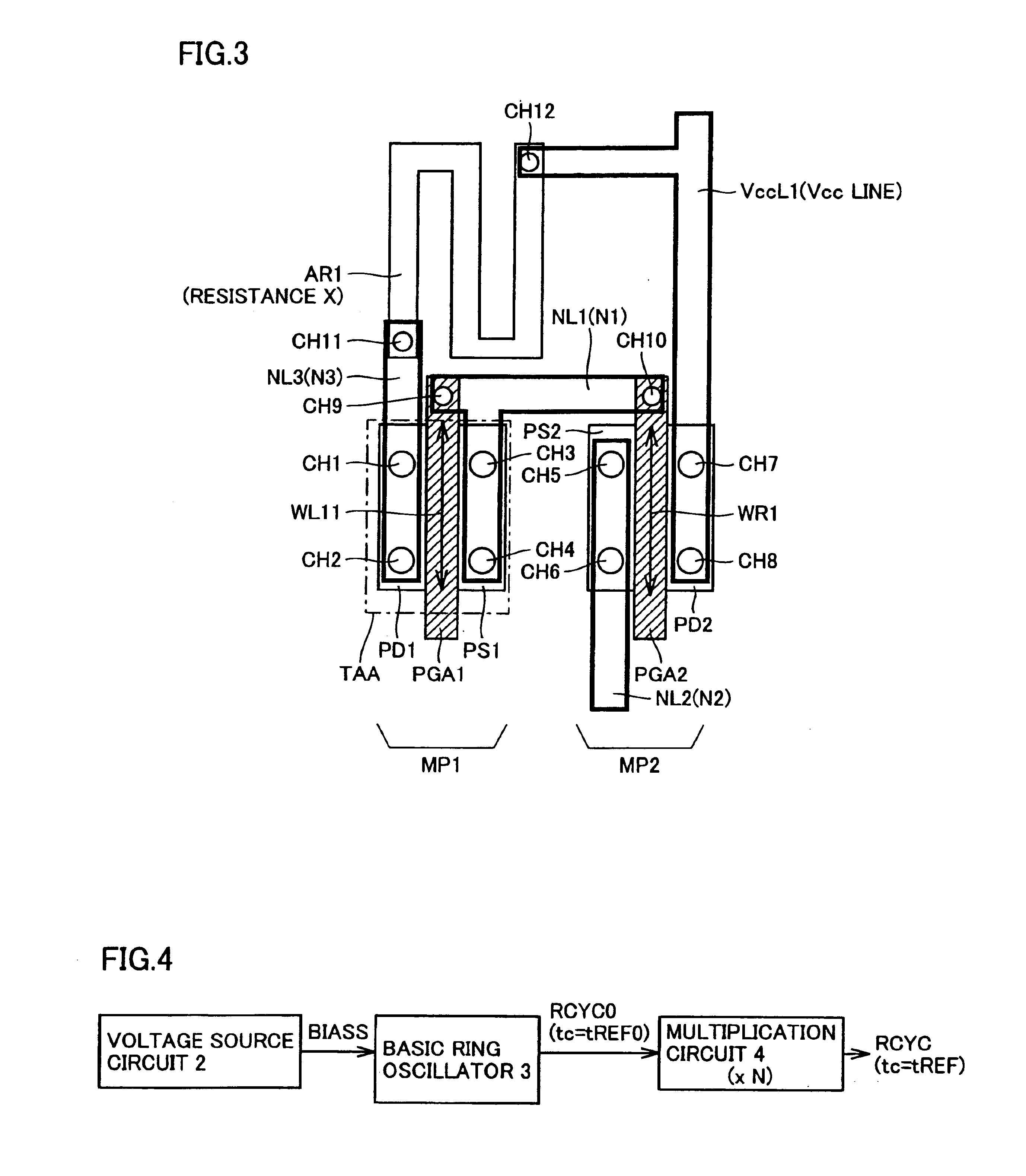
Referring to FIG. 4, a basic ring oscillator 3 is controlled by an output voltage BIASS of a voltage source circuit 2, a transmission signal RCYC0 from basic ring oscillator 3 is multiplied by N by a multiplication circuit 4, and an oscillation frequency RCYC of the refresh timer is thereby determined.

Referring then to FIG. 5, voltage source circuit 2 includes a constant voltage source circuit 5, voltage conversion circuit 1 which inputs output voltage BIASL0 of constant voltage source circuit 5 and which is shown in the first embodiment, and an output voltage generation circuit 6 which inputs output voltage BIASL1 of voltage conversion circuit 1 and which outputs output voltage BIASS.

Constant voltage source circuit 5 is, for example, one shown in FIG. 6 which is normally referred to as a “Weak Inversion type” con...

third embodiment

In the first and second embodiments, an example of the use of one voltage conversion circuit has been described. When the temperature dependency of the output voltage and output current of the voltage conversion circuit is to be increased but only the temperature change of one resistance X is utilized, the selection of the resistance material is limited by the restriction of manufacturing or the like. Therefore, the desired great temperature dependency cannot be sometimes attained.

Considering this, the third embodiment is intended to attain a voltage conversion circuit and a voltage source circuit capable of attaining greater temperature dependency.

Referring to FIG. 9, a voltage source circuit 21 according to the third embodiment is formed by cascading voltage conversion circuit 1 and a voltage conversion circuit 11 to thereby form voltage conversion circuit stages.

It is assumed herein that voltage conversion circuits 1 and 11 are equal to voltage conversion circuit 1 shown in FIG. ...


PUM


Abstract

A semiconductor device according to the present invention has a configuration that a resistance section is connected to only one of a current-mirror section forming a voltage conversion circuit and an output section. With this configuration, it is possible to determine the temperature dependency of an output voltage according to S factors of transistors forming one of the current-mirror section and the output section and a resistance value of the resistance section, and to suppress manufacturing irregularities caused by irregularities of the transistors between the two sections and those among a plurality of resistance materials.

Description

BACKGROUND OF THE INVENTION1. Field of the InventionThe present invention relates to a semiconductor device including a voltage conversion circuit which converts the voltage value of an input voltage according to the change of the resistance value of a resistance section provided in a circuit as temperature changes and which outputs an output voltage.2. Description of the Background ArtRecently, as a portable device such as a cellular phone and a PDA (Personal Digital Assistant) spread widely, the quantities of information processed by these devices rapidly increase. Therefore, the capacity of a work memory is greatly increased and a DRAM (Dynamic Random Access Memory) cell-based semiconductor memory is mainly employed as the work memory.For the portable device driven by a battery, however, the increase of standby current due to a refresh operation which is essential to the DRAM cell is considerably problematic.Meanwhile, the data holding time of a DRAM cell is greatly influenced by...

Claims


Application Information

Patent Timeline
IPC IPC(8): G05F3/16G05F3/08H01L21/822H01L29/00H01L21/70H01L21/8222H01L27/06H03K3/354H01L27/04H03K19/00H03K19/0185H03K3/00H03K19/0948G11C5/14
CPCG11C5/147
Inventor KONO, TAKASHI
Owner RENESAS ELECTRONICS CORP
Why Eureka
Try Eureka