Method for manufacturing tantalum oxy nitride capacitors

a technology of oxy nitride and capacitor, which is applied in the direction of combustible gas purification/modification, separation processes, lighting and heating apparatus, etc., can solve the problem of limiting the size of the capacitor needed for satisfying the required capacitance, and the difficulty of miniaturizing the capacitor, so as to reduce the number of steps, increase the yield, and increase the capacitance of the capacitor

Inactive Publication Date: 2005-02-08
SK HYNIX INC
View PDF8 Cites 15 Cited by
  • Summary
  • Abstract
  • Description
  • Claims
  • Application Information

AI Technical Summary

Benefits of technology

Therefore, a method for manufacturing a tantalum oxy nitride capacitor is disclosed which reduces a number of steps and increases yield by performing the step of doping a MPS (Metastable Poly Silicon) in the same chamber in-situ with the forming of a nitride film before the forming of a tantalum oxy nitride film. The disclosed method prevents the concentration of phosphor contained in the lower electrode from being reduced by removing the phosphor on the surface of the lower electrode in a cleaning process performed between the above two steps, thereby increasing the capacitance of the capacitor.
In a method for manufacturing a capacitor according to the disclosure, since the MPS doping step and a nitride film depositing step before the tantalum oxy nitride film formation are performed in the same chamber, a cleaning process for removing a native oxide is unnecessary, thereby preventing the phenomenon decreasing capacitance of the capacitor and a bridge between cells caused by crushing of MPS particles.
Also, the tantalum oxy nitride postprocessing step can be, performed by nitrating the surface under NH3 (or N2 / H2, N2O, O2) atmosphere at a temperature ranging from about 200 to about 600° C. by using plasma or nitrifying the same under N2O (or O2) atmosphere. By performing the postprocessing step as above, structural defects such as a micro crack and a pin hole on an interface can be reinforced and homogeneity can be improved. Although the characteristic of the tantalum oxy nitride is improved by this method, a process is added and therefore this step can be omitted if the electrical characteristic needed to a product is obtained in the high temperature heat treatment of the next step. Particularly, after depositing an amorphous tantalum oxy nitride thin film, in case of using a RTP (rapid thermal process) or an electric furnace, crystallization can be induced by a process for nitrating or oxidizing the resultant material for a time period ranging from about 30 seconds to about 120 minutes at a temperature ranging from about 650 to about 950° C. under a NH3 (or N2 / H2, N2O, O2) atmosphere.

Problems solved by technology

However, there is a limit to the size needed for storing charge for satisfying a required capacitance.
Thus, there occurs a difficulty in miniaturizing the capacitor.
Due to the increase in temperature caused by the plasma, a problem occurs in that a tantalum oxy nitride film deposited by the low pressure chemical vapor deposition (LPCVD) is deposited non-uniformly in the wafer and thus it is difficult to meet process requirements.
Particularly, it is necessary that the tantalum oxy nitride film be deposited at a low temperature of below 450° C., so the problem caused by the increase in temperature may become more serious.
In addition, in the cleaning process between the MPS doping step and the nitride film processing step of the process for preprocessing tantalum oxy nitride, the concentration of phosphor contained in the lower electrode may be reduced by removing highly doped phosphor by the MPS doping, which may lead to depletion and thus reduce the capacitance of the capacitor.

Method used


Image

  • Method for manufacturing tantalum oxy nitride capacitors
  • Method for manufacturing tantalum oxy nitride capacitors
  • Method for manufacturing tantalum oxy nitride capacitors

Examples


Embodiment Construction

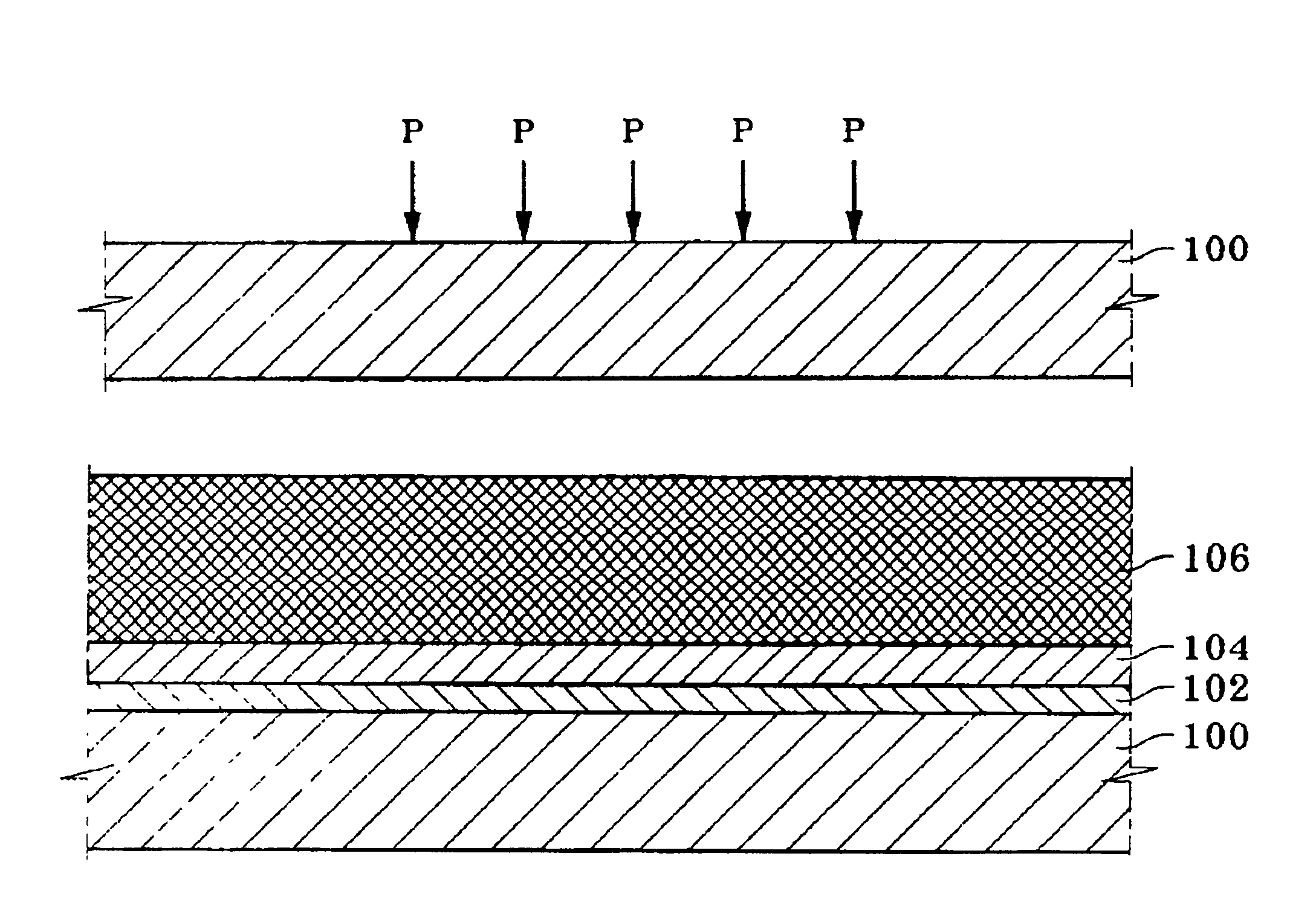
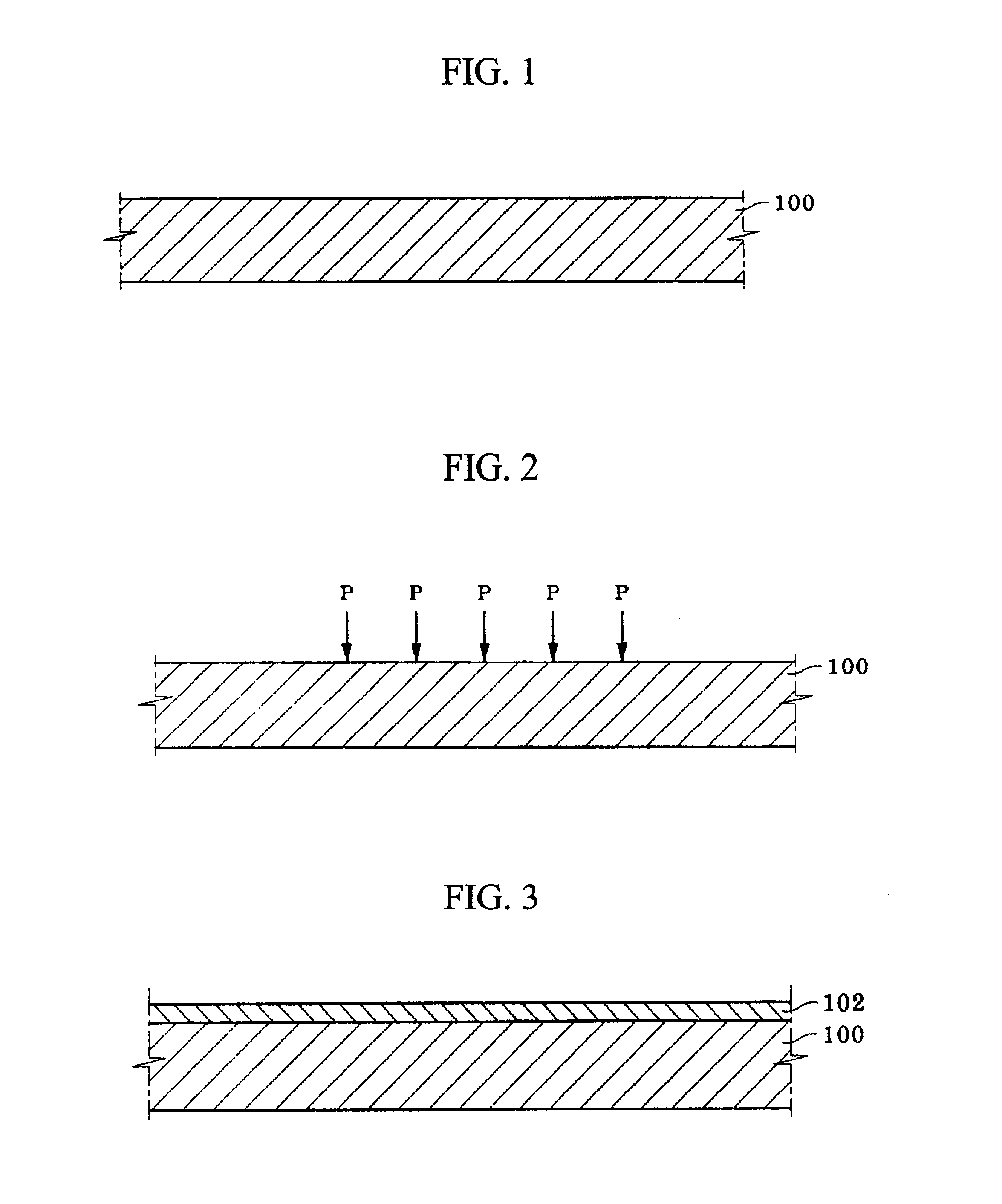
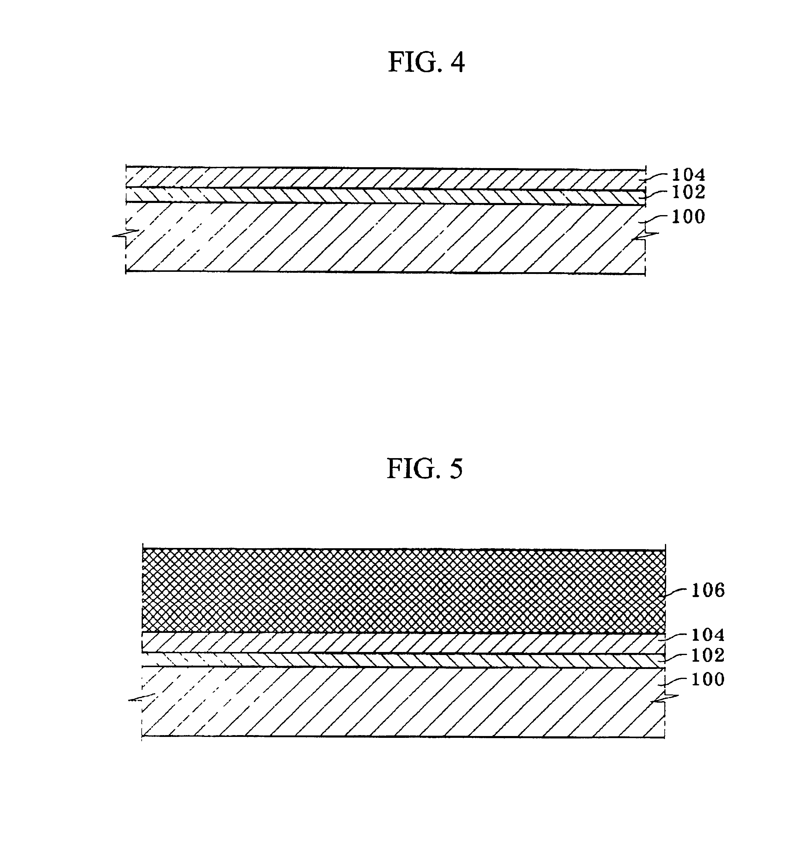
FIGS. 1 through 5 are views illustrating the disclosed sequence of processes for manufacturing a tantalum oxy nitride capacitor.

In process accord to the disclosure, as illustrated in FIG. 1, a lower electrode 100 is formed on the surface of a semiconductor substrate 40 (not shown). At this time, the lower electrode is selected from undoped silicon, low doping silicon or doped / undoped silicon which are capable of MPS growth. At this time, a thin film used as the electrode is an amorphous silicon film deposited at a temperature of below about 560° C. by using a gas containing a silicon source such as SiH4, Si2H6, SiH2Cl2 and the like and a gas containing PH3 such as PH3 / N2, PH3 / SiH4, PH3 / Ar and the like. At this time, conditions such as an amount of gas, pressure, etc. can be made suitable for a selective polycrystalline silicon growing technique (MPS growing technique).

Next, the thusly formed lower electrode is wet / dry etched by using a mixture of gases such as HF / H2O, HF / H2O2, BOE, ...


PUM

PropertyMeasurementUnit
temperatureaaaaaaaaaa
pressureaaaaaaaaaa
temperatureaaaaaaaaaa

Abstract

A method for manufacturing a capacitor using a tantalum oxy nitride (TaON) film in a process for a semiconductor device. More particularly, a method for manufacturing a capacitor which reduces a number of steps and thus increases yield by in-situ performing P-doping after forming a MPS (Metastable Poly Silicon) on a lower electrode and forming a nitride film before forming a tantalum oxy nitride film to prevent the concentration of phosphor contained in the lower electrode from being reduced by removing the phosphor on the surface of the lower electrode in a cleaning process between the above two steps, for thereby increasing the capacitance of the capacitor.

Description

BACKGROUNDTechnical FieldA method for manufacturing a capacitor with a tantalum oxy nitride (TaON) film for a semiconductor device is disclosed. More particularly, a method for manufacturing a capacitor is disclosed with a reduced number of steps and thus an increased yield by in-situ performing the step of executing P-doping after forming a MPS (Metastable Poly Silicon) on a lower electrode and the step of forming a nitride film before forming a tantalum oxy nitride film. The disclosed method prevents the concentration of phosphor contained in the lower electrode from being reduced by removing the phosphor on the surface of the lower electrode in a cleaning process performed between the above two steps, thereby increasing the capacitance of the capacitor.DESCRIPTION OF THE RELATED ARTGenerally, a capacitor stores a charge required for the operation of a semiconductor. As the semiconductor device is highly integrated, the size of a cell decreases, while the capacitance required for ...

Claims


Application Information

Patent Timeline
Patent Type & Authority Patents(United States)
IPC IPC(8): H01L21/02H01L21/314H01G4/33H01L21/318H01L21/822H01L21/8242H01L27/04H01L27/108
CPCH01L21/3144H01L28/40Y10T29/435Y10T29/43Y10T29/417Y10T29/49128H01L21/02271H01L21/02183H10B99/00H01L21/02356H01L21/0234
Inventor PARK, DONG-SUJEON, KWANG-SEOK
Owner SK HYNIX INC
Why Eureka
Try Eureka