Electron beam system and method of manufacturing devices using the system

a technology of electron beam and manufacturing device, applied in the field of electron beam system, can solve the problems of difficult evaluation of samples with high throughput, poor s/n ratio, large shot noise of electron beam, etc., and achieve the effect of small shot noise and higher beam curren

Inactive Publication Date: 2005-02-08
EBARA CORP
View PDF12 Cites 23 Cited by
  • Summary
  • Abstract
  • Description
  • Claims
  • Application Information

AI Technical Summary

Benefits of technology

The present invention has been made to solve the problems pointed out above, and the object thereof is to provide an electron beam system which comprises an axisymmetric filter as well as an electron gun with a smaller shot noise, and allows a relatively higher beam current to be obtained as compared to that which can be achieved by using an electron gun with the same brightness, and also to provide a defect inspection method using the same electron beam system, as well as a device manufacturing method using the same electron beam system and defect inspection method.
There has been a problem that if both rough alignment and fine alignment are carried out, it takes a long time to complete an alignment operation, resulting in a lower throughput (a quantity of processing per unit time) achieved by the inspection apparatus. In addition, when an electron optical system is used to conduct alignment, an electron beam dose equivalent to or greater than that applied in the sample evaluation would be applied to the wafer, which in turn could destroy a gate oxide or the like. The present invention is also directed to solving the above problem. Accordingly, another object of the present invention is to provide an inspection apparatus, in which inspection of a wafer can be carried out by conducting alignment without using any electron beams, and thus without destroying the gate oxide and the like. Another object of the present invention is to provide a device manufacturing method using such an inspection apparatus as described above.

Problems solved by technology

However, it is problematic that although in a schottky electron gun, a beam current three to ten times higher as compared to that obtained by a thermionic emission electron gun (e.g., LaB6 electron gun) can be obtained, and a shot noise of the electron beam is quite large and inevitably an S / N ratio is not so good, which makes it difficult to evaluate a sample with high throughput.
On the other hand, the crossover image demagnification type beam by using the LaB6 electron gun also has a drawback such that it is impossible to make the beam current higher, and this makes it difficult to evaluate a sample with high throughput.
It is also problematic that the space charge effect becomes greater in proportion to the length of the optical path, and it is difficult to accomplish a good intensity and position stability of the electron beam.

Method used


Image

  • Electron beam system and method of manufacturing devices using the system
  • Electron beam system and method of manufacturing devices using the system
  • Electron beam system and method of manufacturing devices using the system

Examples


fourth embodiment

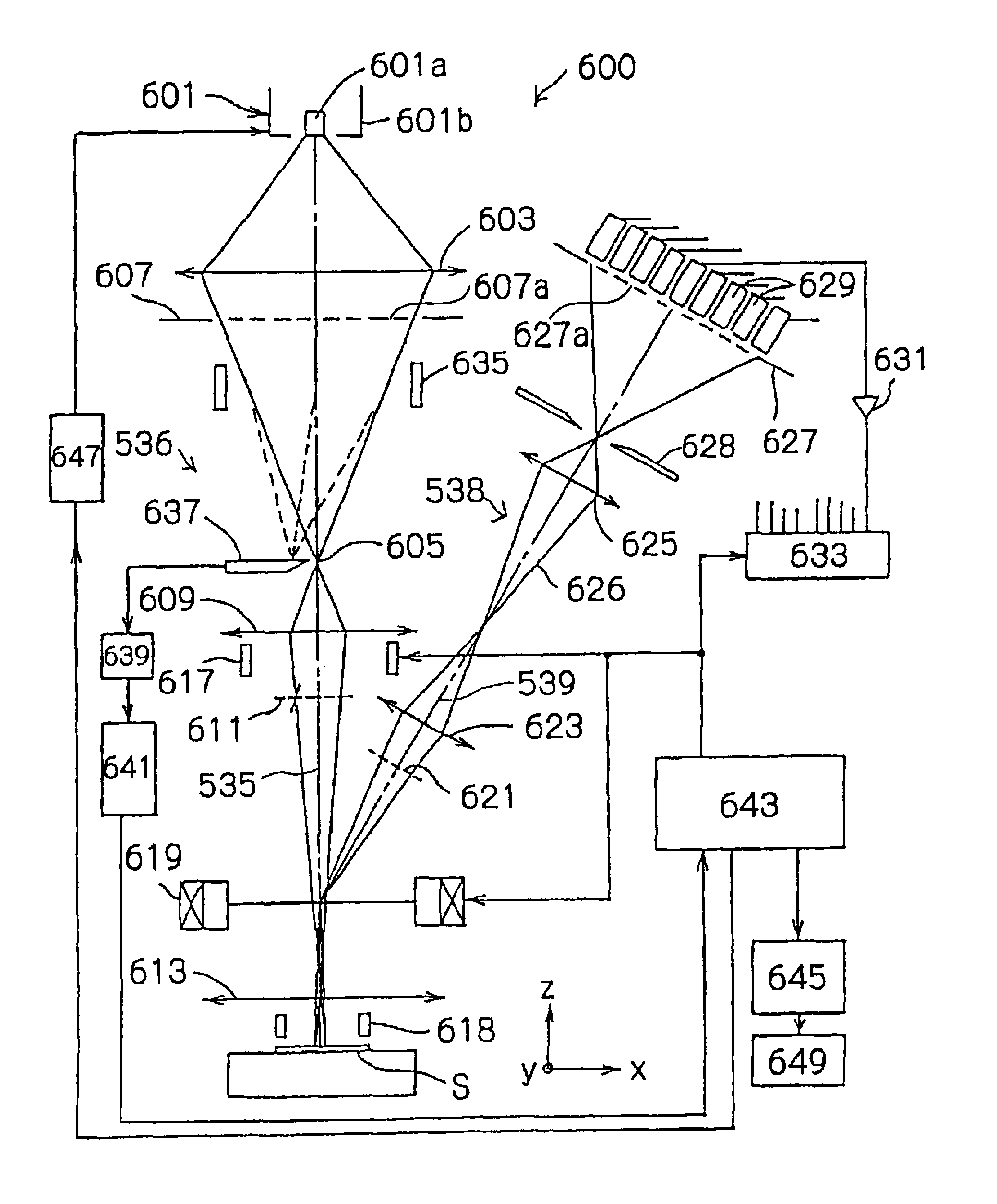
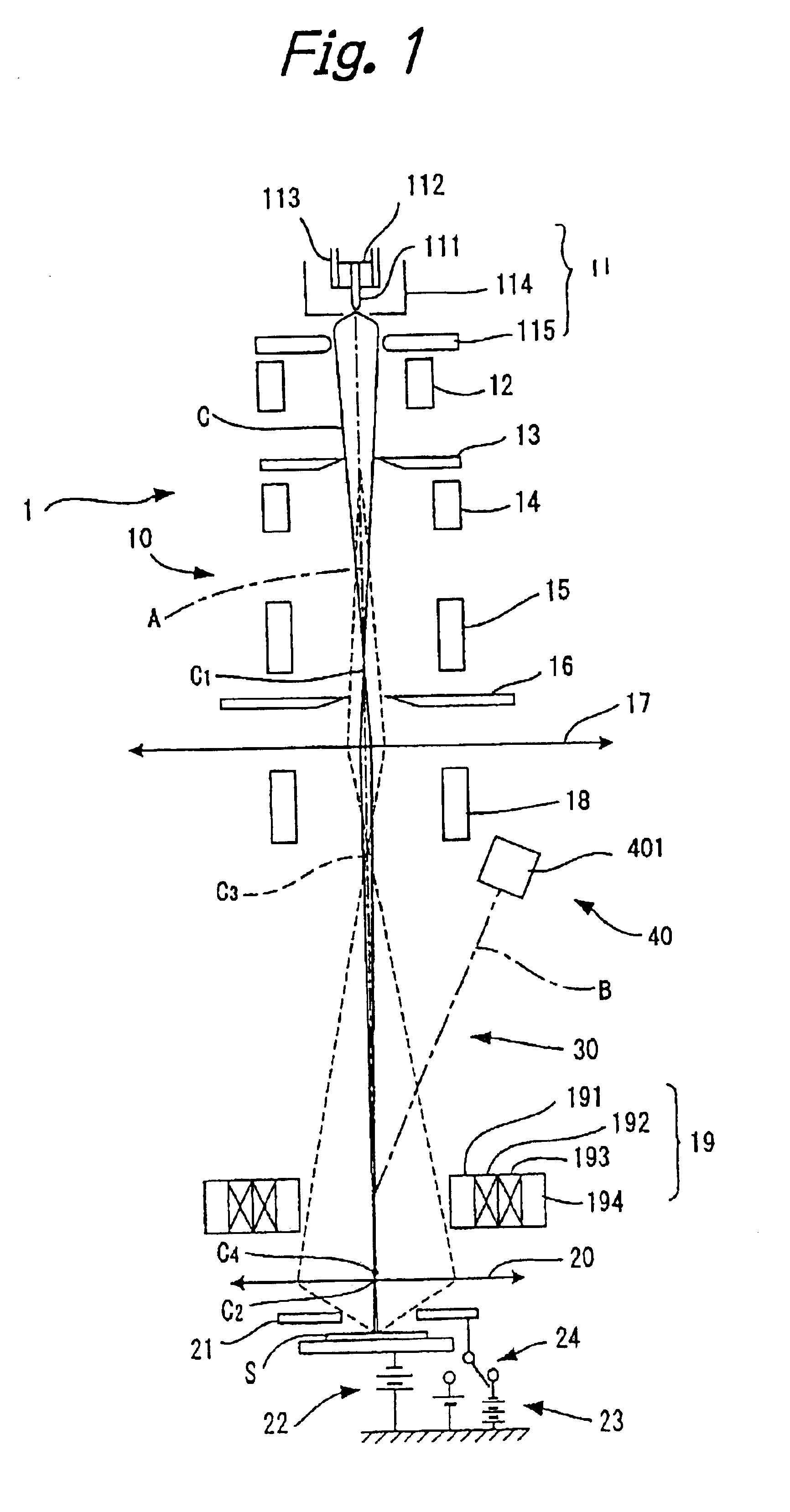
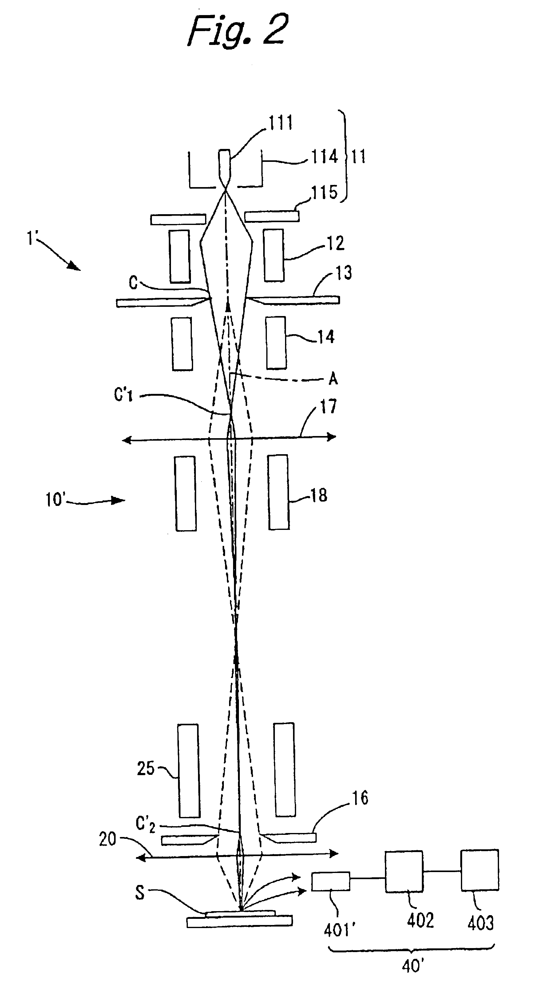
In the present invention, defect inspection is carried out by using the electron beam system comprising the electron optical system shown in FIG. 3, in which, for example, a electric resistance of a via connection with a lower-layer wiring may be evaluated, said via being used to connect the lower-layer wiring and an upper-layer wiring in a multi-layered wiring sample. Evaluating the electric resistance of the via connection with the lower-layer wiring takes advantage of such a characteristic that when the charge is given to the surface of the sample, if the lower-layer wiring is grounded or almost grounded and the electric resistance between the via connection and the lower-layer wiring is sufficiently small, then the via may immediately return back to the ground potential, but if the electric resistance between the via connection and the lower-layer wiring is great, then the via may be charged to positive. Accordingly, measuring the surface potential immediately after the injectio...


PUM

PropertyMeasurementUnit
widthaaaaaaaaaa
widthaaaaaaaaaa
electrode potential biasaaaaaaaaaa

Abstract

An electron beam system wherein a shot noise of an electron beam can be reduced and a beam current can be made higher, and further a shaped beam is formed by a two-stage lenses so as to allow for an operation with high stability. In this electron beam system, an electron beam emitted from an electron gun is irradiated onto a sample and secondary electrons emanated from the sample are detected. The electron gun is a thermionic emission type and designed to operate in a space charge limited condition. A shaping aperture and a NA aperture are arranged in front locations of the electron gun. An image of the shaping aperture formed by an electron beam emitted from the thermionic emission electron gun is focused onto a surface of the sample through the two-stage lenses.

Description

BACKGROUND OF THE INVENTIONThe present invention relates to an electron beam system, a defect inspection apparatus for a device, which employs the same electron beam system, and a manufacturing method of a device using the same defect inspection apparatus, and more specifically, relates to an electron beam system which can evaluate a sample (a semiconductor wafer) having a device pattern with a minimum line width equal to or less than 0.1 μm with both a high throughput and high reliability, a defect inspection apparatus for a device, which employs the same electron beam system, and a manufacturing method of a device which can improve a yield thereof by evaluating a wafer after it has been processed using the same defect inspection apparatus.The present invention also relates to an electron beam system and a defect inspection method for evaluating a device, such as a wafer or a mask, having a pattern with a minimum line width in a range of 0.1 micron, and also to a method for manufac...

Claims


Application Information

Patent Timeline
Patent Type & Authority Patents(United States)
IPC IPC(8): G01N23/04G01N23/02G21K7/00H01J37/28
CPCG01N23/04H01J37/28H01J2237/2817G01N23/2251
Inventor NAKASUJI, MAMORUKATO, TAKAOSATAKE, TOHRUWATANABE, KENJIMURAKAMI, TAKESHINOJI, NOBUHARU
Owner EBARA CORP
Why Eureka
Try Eureka