Driving circuit for light emitting element, and optical communication device using same

a technology driving circuits, applied in electromagnetic transmission, electromagnetic transceivers, transmission, etc., can solve the problems of deteriorating yield of optical communication apparatuses of higher speed, inability to adjust compensation amounts, uneven production of finished products of light emitting elements 2, etc., and achieve the effect of stably obtaining

Inactive Publication Date: 2005-03-01
SHARP KK
View PDF8 Cites 9 Cited by
  • Summary
  • Abstract
  • Description
  • Claims
  • Application Information

AI Technical Summary

Benefits of technology

With the above arrangement, it is possible to stably obtain the output light having the duty ratio equal to that of the input signal always.

Problems solved by technology

However, finished products of the light emitting element 2 have production unevenness among them in terms of its light emission delay time (a length of time of the delay in the light emission).
Therefore, in case where the low-pass filter is integrated on the integrated circuit, there is a drawback that the compensation amount cannot be adjusted.
Therefore, if the adjustment of the compensation amount is impossible as previously discussed, it is a problem that an optical communication apparatus of higher speed cannot be realized without deteriorating its yield.
Moreover, if a resistor r or a capacitor c of the low-pass filter for the adjustment of the compensation amount is mounted externally on the integrated circuit, a line for the signal s2 is exposed out of the integrated circuit, thus being more susceptible to disturbance noise.
Thus, this arrangement has a poor jitter property of the signals.
However, it is a drawback that such large time constant makes the jitter larger because the jitter depends on signal frequencies.

Method used


Image

  • Driving circuit for light emitting element, and optical communication device using same
  • Driving circuit for light emitting element, and optical communication device using same
  • Driving circuit for light emitting element, and optical communication device using same

Examples


Embodiment Construction

Described below is an embodiment of the present invention, with reference to FIGS. 1 to 4.

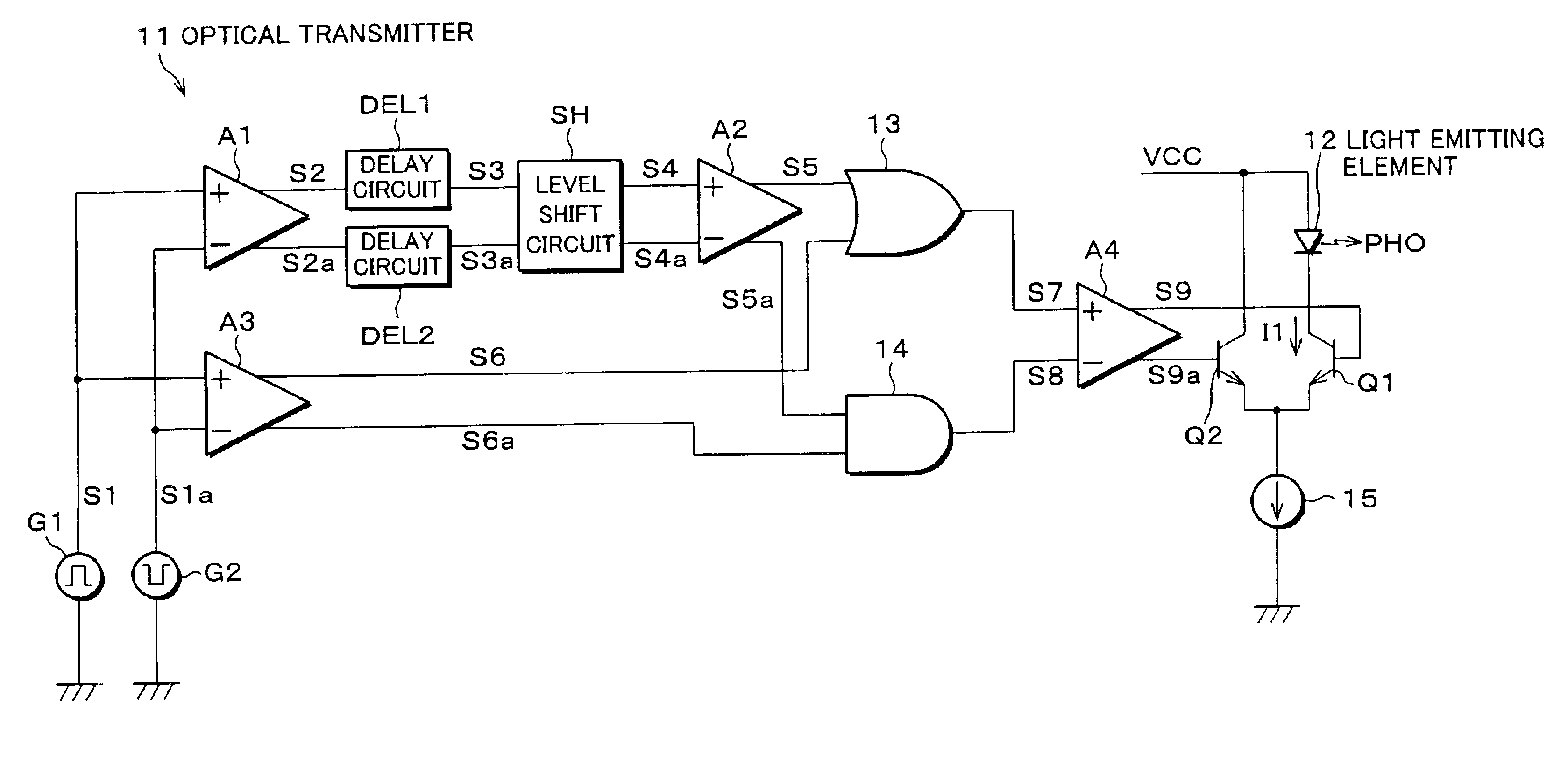
FIG. 1 is a block diagram illustrating an electric arrangement of an optical transmitter 11, which is a driving circuit of an embodiment of the present invention. The optical transmitter 11 is suitable as an optical communication device for use in a system (so called OP iLINK) in which, instead of a metal wire, an optical fiber is used as a transmission line, which a physical layer in conformity with IEEE1394-1995 and IEEE1394a-2000. Moreover, the optical transmitter 11, which is capable of driving a semiconductor laser or a light emitting diode as a light emitting element 12, is especially suitable for driving a light emitting diode that emits light with a large delay.

Signal sources G1 and G2 respectively outputs differential input signals S1 and S1a suitable for high-speed transmission. The input signals S1 and S1a are supplied to a buffer amplifier A1 for amplifying the difference between th...


PUM


Abstract

A delay circuit delays an input signal. Further, a level shift circuit, which has a variable level shift amount, is provided between the delay circuit and an OR circuit, thereby making it possible to adjust a time during which a logic of active of the delayed signal is kept. Moreover, the OR circuit performs an OR operation of the input signal and an output signal of the level shift circuit so as to obtain a signal of an OR logic, which drives a light emitting element. With this arrangement, the level shift amount is adjusted in response to a control signal externally supplied, in an optical transmitter arranged such that the input signal and output light emitted from the light emitting element with a delay in the emission, have the equal duty ratio. In this way, property unevenness among finished products of the light emitting element is cancelled out. Thus, it is possible to drive the light emitting element at a higher speed.

Description

FIELD OF THE INVENTIONThe present invention relates to a driving circuit for a light emitting element for use in an optical communication and in recording / reproduction of an optical recording medium, especially to a driving circuit for a light emitting element that is suitably used for short distance data communication using a light emitting element having a large delay in the light emission, and an optical communication device using the same.BACKGROUND OF THE INVENTIONFIG. 7 is a block diagram illustrating an electric arrangement of an optical transmitter 1, which is a typical driving circuit in the prior art. The optical transmitter 1 is shown in FIG. 9 of Japanese Publication of Patent, Tokukouhei, No. 4-64216 (published on Oct. 14, 1992). The optical transmitter 1 drives a light emitting element 2, which is a semiconductor laser or a light emitting diode. An input signal s1 is supplied from a signal source 3 to a buffer amplifier 4, which amplifies a difference between the input...

Claims


Application Information

Patent Timeline
Patent Type & Authority Patents(United States)
IPC IPC(8): H04B10/155H04B10/152H04B10/07H01L33/00H04B10/2507H04B10/40H04B10/50H04B10/564H04B10/58H04B10/60
CPCH04B10/504
Inventor SHIMIZU, TAKAYUKI
Owner SHARP KK
Why Eureka
Try Eureka