Apparatus for fabricating thin-film semiconductor device

a thin-film semiconductor and apparatus technology, applied in semiconductor devices, chemical vapor deposition coatings, coatings, etc., can solve the problems of contaminant adhesion to the surface, degradation of the performance of resultant tft, and difficulty in keeping a chamber located at the core, so as to prevent contaminants and reduce the concentration of contaminants

Inactive Publication Date: 2005-03-08
GOLD CHARM LTD
View PDF30 Cites 44 Cited by
  • Summary
  • Abstract
  • Description
  • Claims
  • Application Information

AI Technical Summary

Benefits of technology

[0045]In contrast, in accordance with the present invention, highly purified oxygen gas is introduced into a chamber just after silicon has been crystallized by laser beams, to thereby form a natural oxidation film having a low concentration of contaminants. By forming such a natural oxidation film on a surface of silicon, it would be possible to prevent contaminants from being adhered to a surface of silicon in various chambers such as a chamber in which laser beam is radiated, a chamber through which a substrate is transferred to another chamber, or a chamber in which a film is formed.
[0046]If active gases such as radicals or ions are used for formation of a natural oxidation film, it would be possible to effectively form a natural oxidation film and establish hydrogen passivation. However, the use of those active gases might cause absorption of contaminants adhered to a wall of a chamber into a natural oxidation film, and thus, it is not preferable to use such active gases.

Problems solved by technology

Since a surface of silicon formed by laser crystallization is quite active, contaminants are likely to be adhered to the surface, if the silicon is exposed to atmosphere.
This results in degradation in performances of resultant TFT.
That is, there is a problem of insufficiency in performances of a silicon film (or a trap level density) in order to have sufficient cleanness in a product having a silicon film and a gate insulating film both formed without exposure to atmosphere in the same apparatus.
Hence, it is quite difficult to keep a chamber located at a core, away from contaminants.
There occurs cross-contamination in transfer of a substrate between chambers, even though the cross-contamination is slight.
For instance, an in-line type apparatus suggested in Japanese Unexamined Patent Publication No. 5-182923 is accompanied with a problem that it is unavoidable generation of minute dust, in particular, metal particles due to a great frictional area between parts in vacuum.
For instance, if silicon is coated with active species having energy, for instance, radical species such as hydrogen radical, oxygen radical, hydrogen ion, oxygen ion, ion species or ozone, after the silicon has been crystallized by laser beam, but before a gate insulating film is formed, contaminants adhered to a wall of a chamber and metal constituting a wall of a chamber are excited, resulting in that atmosphere in which a substrate is put is contaminated.
The fourth problem is that since laser radiation in oxidation atmosphere reflects dispersion in laser intensity in a step of introducing oxygen into silicon, there would be dispersion in a concentration of oxygen in a silicon film.
This results in non-uniformity in characteristics of resultant silicon films.
When a plurality of steps are to be successively carried out without exposure to atmosphere, for instance, steps of crystallizing a silicon film by means of laser beam and thereafter forming a gate insulating film, though it is possible to reduce contaminants adhered to the silicon film by not exposing the silicon film to atmosphere, the above-mentioned problems still interfere with fabrication of a semiconductor device.
However, this advantage of accomplishing such low densities is restricted to performances of a silicon film.
However, silicon particles separated from a silicon film during laser radiation are adhered to a window through which laser beam is introduced into the apparatus, resulting in reduction in a laser transmission rate with the lapse of time.
However, in this apparatus, since a laser beam which is usually focused on a surface of a substrate is focused on a surface of the window having a different optical length, it would be absolutely necessary to rearrange optical systems.
When there are employed optical systems having a small focal length, in particular, when mask projection method is carried out, it is necessary to accurately position optical systems, resulting in reduction in an operation efficiency of the apparatus.

Method used


Image

  • Apparatus for fabricating thin-film semiconductor device
  • Apparatus for fabricating thin-film semiconductor device
  • Apparatus for fabricating thin-film semiconductor device

Examples


Embodiment Construction

, in which like reference characters designate the same or similar parts throughout the drawings.

BRIEF DESCRIPTION OF THE DRAWINGS

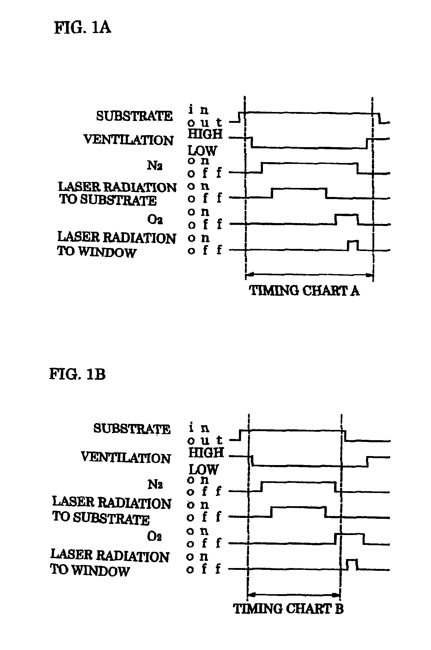
[0081]FIG. 1A is a timing chart of processing a substrate in a method in accordance with the embodiment of the present invention.

[0082]FIG. 1B is another timing chart of processing a substrate in a method in accordance with the embodiment of the present invention.

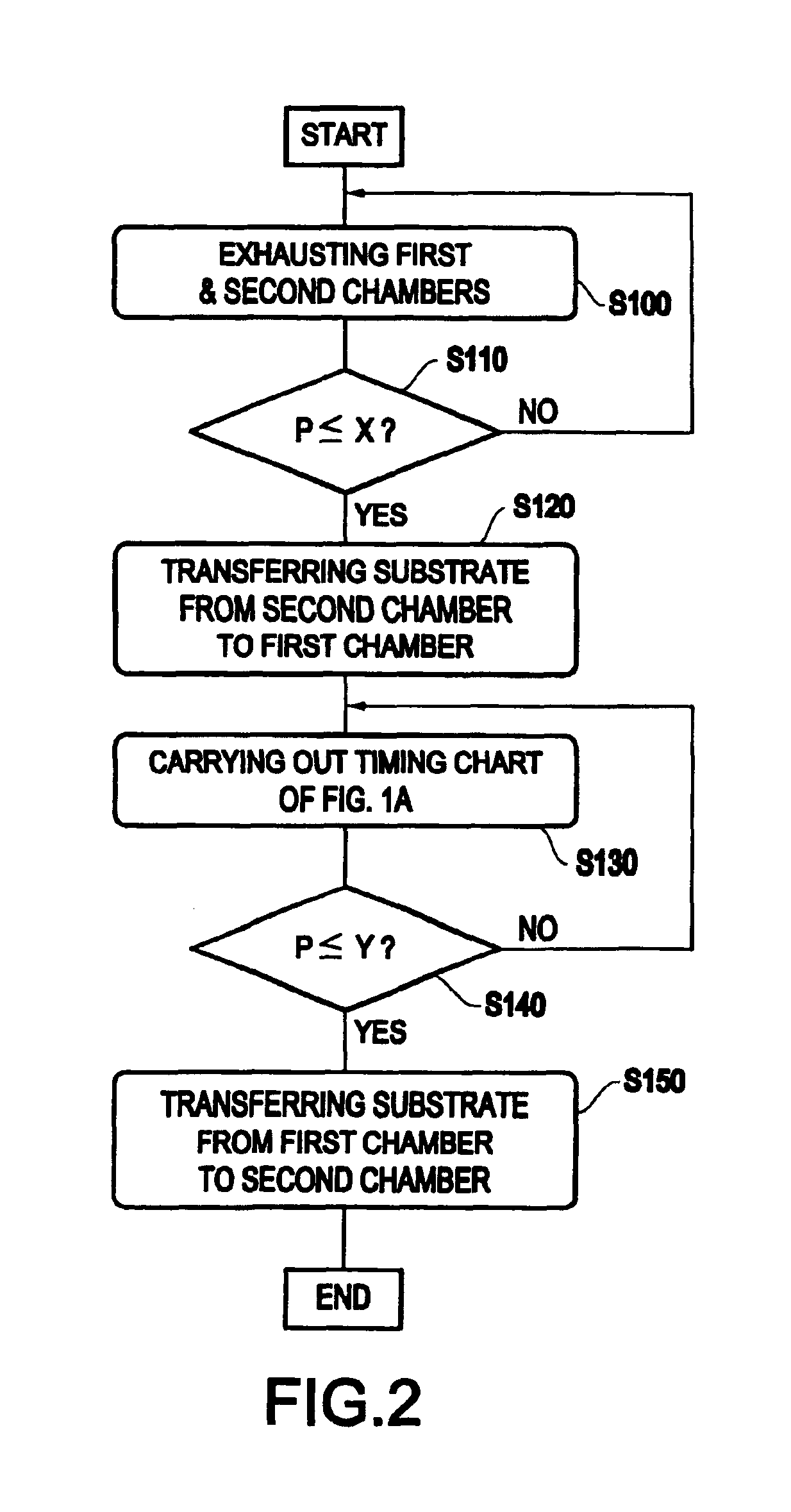
[0083]FIG. 2 is a flow-chart of processing a substrate in a method in accordance with the embodiment of the present invention.

[0084]FIG. 3 is another flow-chart of processing a substrate in a method in accordance with the embodiment of the present invention.

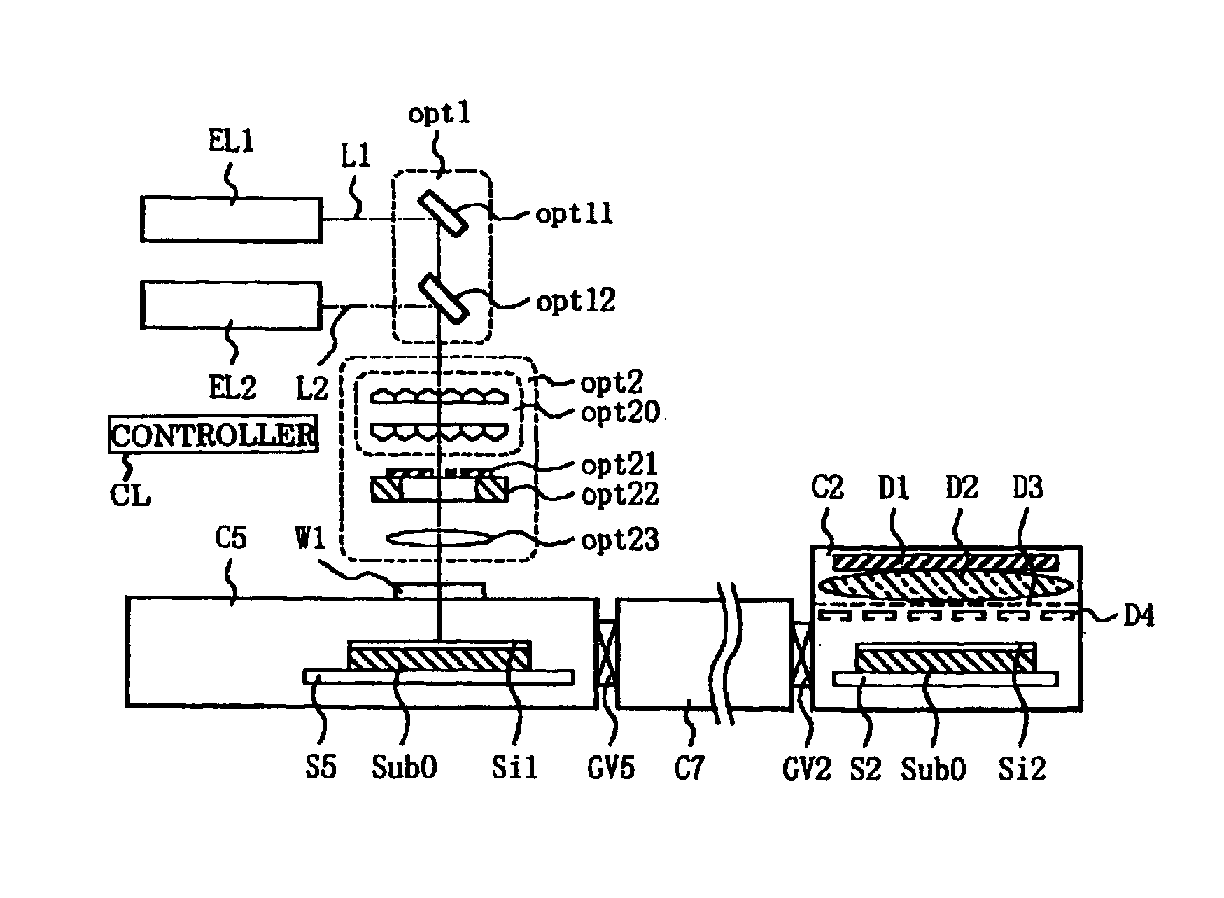
[0085]FIG. 4 is a cross-sectional view of an apparatus of forming a thin-film semiconductor device in accordance with the embodiment of the present invention.

[0086]FIG. 5 is a cross-sectional view of another apparatus of forming a thin-film semiconductor device in accordance with the embodiment of the present invention.

[0087]FIG. 6 is a top vi...


PUM

PropertyMeasurementUnit
temperatureaaaaaaaaaa
boiling pointaaaaaaaaaa

Abstract

There is provided a method of fabricating a thin-film semiconductor device, including the steps of (a) melting and recrystallizing at least a surface of a thin semiconductor film formed on a substrate, in a pressure lower than an atmospheric pressure or in inert gas atmosphere, (b) keeping the substrate in atmosphere including oxygen gas, and (c) forming an insulating film on the thin semiconductor film with the substrate being kept in a pressure lower than an atmospheric pressure or inert gas atmosphere.

Description

[0002]The present Application is a Divisional Application of U.S. patent application Ser. No. 09 / 615,058, filed on Jul. 12, 2000, now U.S. Pat. No. 6,642,091.BACKGROUND OF THE INVENTION[0003]1. Field of the Invention[0004]The invention relates to a method of fabricating a thin-film semiconductor device and an apparatus for fabricating the same, and more particularly to a method of forming a thin silicon film used for a crystalline silicon thin-film transistor, and an interface between semiconductor and an insulating film, used for a field effect transistor, and further to an apparatus of fabricating such a thin silicon film and such an interface.[0005]2. Description of the Related Art[0006]Japanese Patent Publication No. 7-118443 has suggested a method including the step of radiating laser beam having a short wavelength, to an amorphous silicon thin film formed on an amorphous substrate, to thereby fabricate a thin film transistor. The method makes it possible to crystallize amorpho...

Claims


Application Information

Patent Timeline
Patent Type & Authority Patents(United States)
IPC IPC(8): C23C16/56H01L21/20H01L21/02H01L21/336H01L21/00
CPCC23C16/56H01L21/2026H01L29/66757H01L21/67253H01L21/67069H01L21/02683H01L21/02422H01L21/02488H01L21/02496H01L21/02505H01L21/0242H01L21/0262H01L21/02686H01L21/02491H01L21/02532H01L21/02691H01L21/0268
Inventor TANABE, HIROSHI
Owner GOLD CHARM LTD
Why Eureka
Try Eureka