

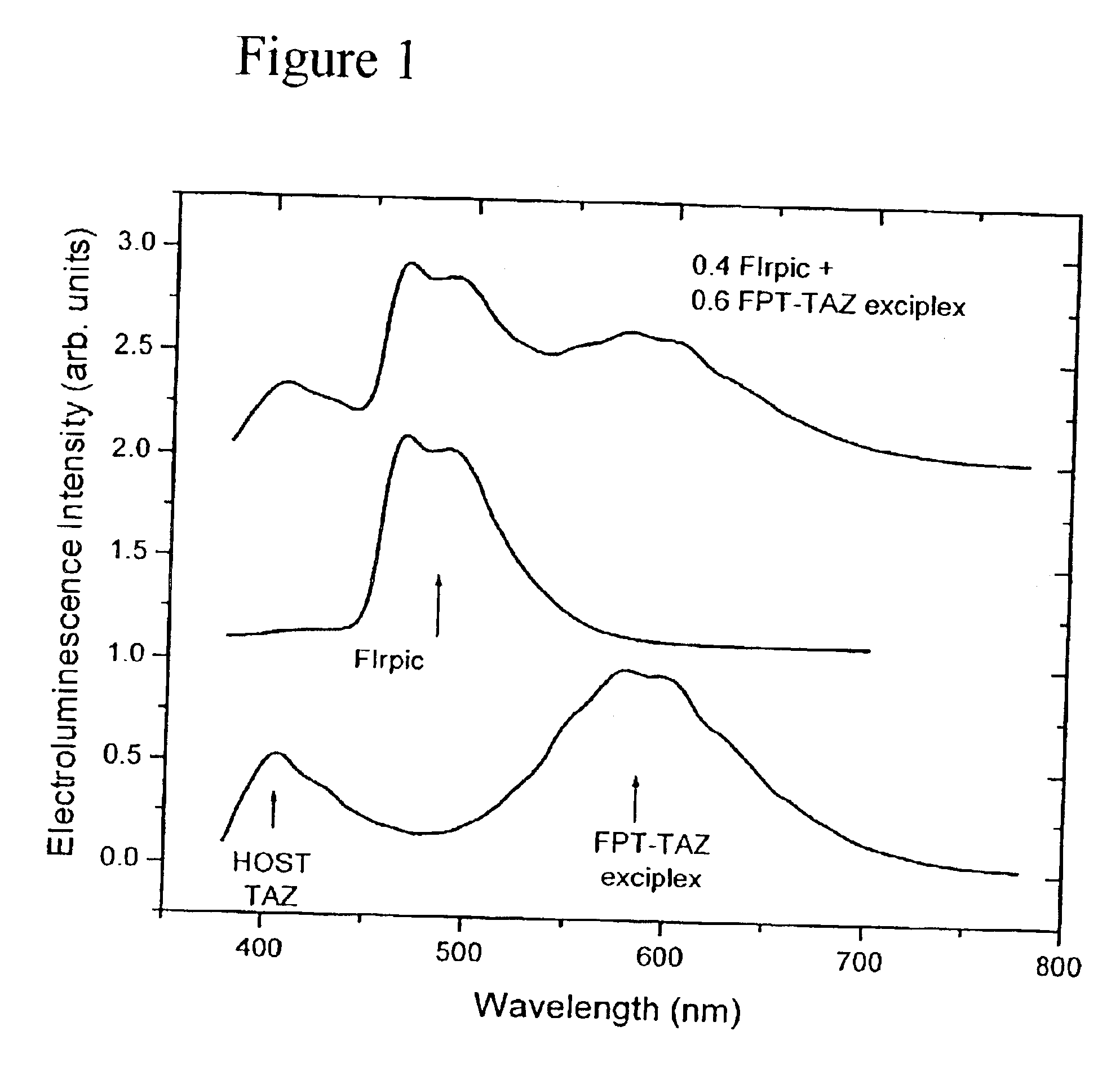
White light emitting OLEDs from combined monomer and aggregate emission
a light-emitting oled and monomer technology, applied in the field of white-emitting oleds, or woleds, can solve the problems of inability to convert excitons into higher-energy singlet excited states, energy loss, decay process, etc., and achieves simple, bright and efficient, high color rendering index
- Summary
- Abstract
- Description
- Claims
- Application Information
AI Technical Summary
Benefits of technology
Problems solved by technology
Method used
Image

Examples
example 1
The electrophosphorescent excimer WOLEDs were grown on a glass substrate pre-coated with an indium-tin-oxide (ITO) layer having a sheet resistance of 20-W / sq. Prior to organic layer deposition, the substrates were degreased in ultrasonic solvent baths and then treated with an oxygen plasma for 8 min. at 20 W and 150 mTorr. Poly(ethylene-dioxythiophene):poly(styrene sulphonic acid) (PEDOT:PSS), used to decrease OLED leakage current and to increase fabrication yield, was spun onto the ITO at 4000 rpm for 40 s, and then baked in vacuum for 15 min at 120° C., attaining an approximate thickness of 40 nm. The hole transporting and host materials, as well as the two dopants were prepared by standard procedures (See Lamansky, S. et al., Inorg. Chem. 40, 1704-1711, 2001) and purified by thermal gradient vacuum sublimation. The molecular organic layers were sequentially deposited without breaking vacuum by thermal evaporation at a base pressure of <8×10⁻⁷ Torr.
Deposition began with a 30 ...
example 2
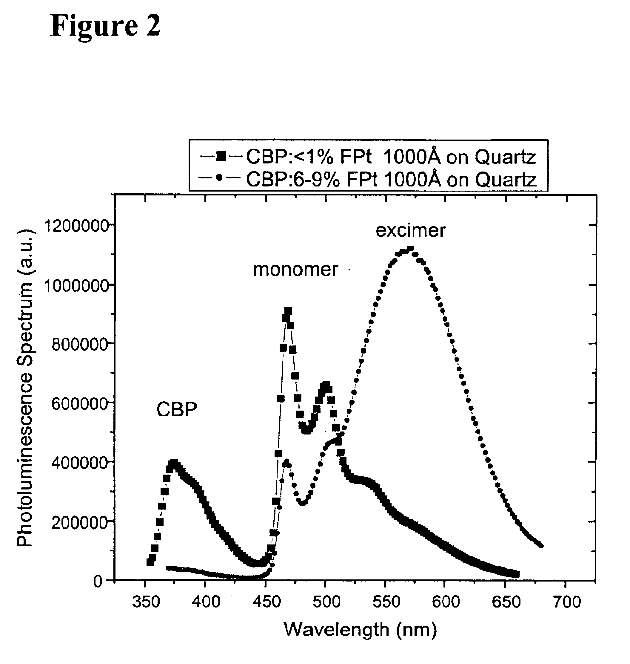
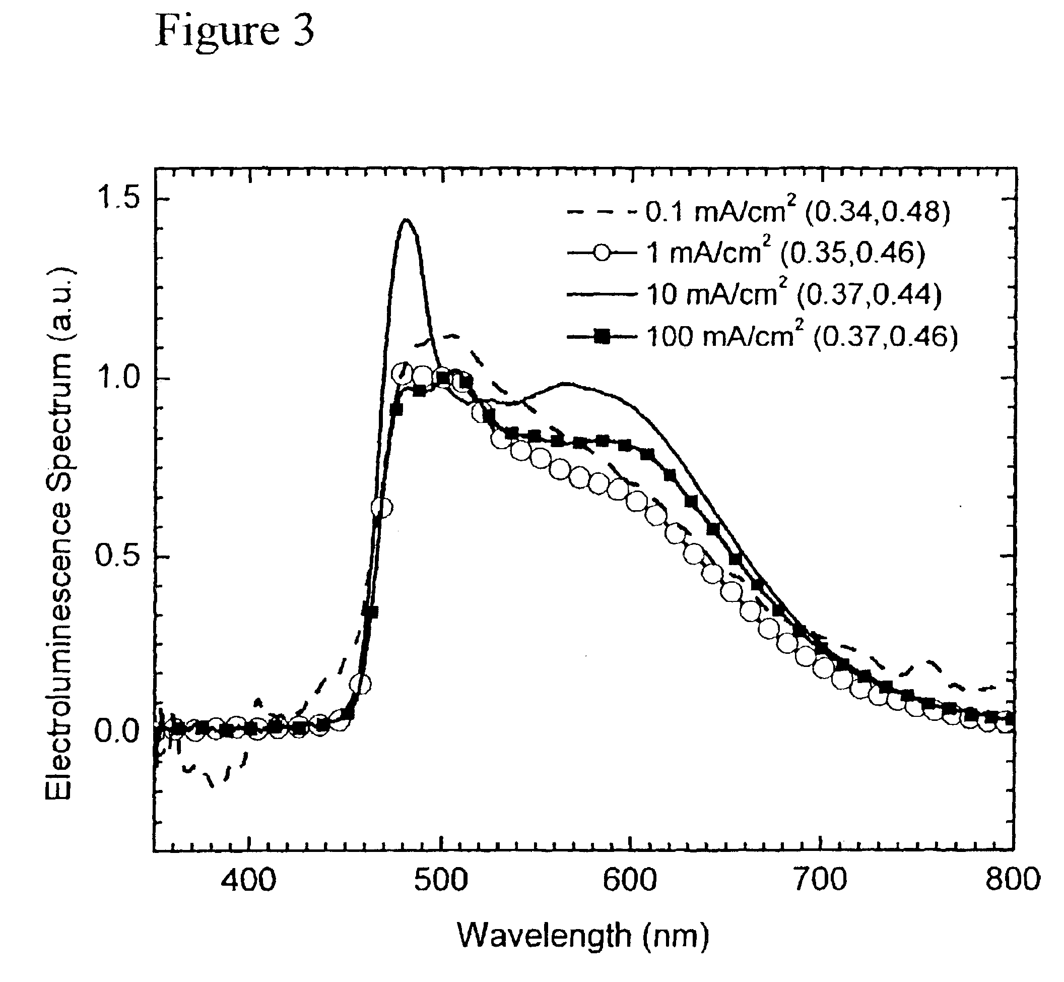
OLEDs were prepared with FPt3 at doping levels of 8, 10 and 12%. The device structure consisted of ITO / NPD (400 Å) / Ir(ppz)3 (200 Å) / CBP-FPt3 (300 Å) / BCP (150 Å) / Alq3 (200 Å) / Mg-Ag. The current voltage characteristics of the-three devices were similar, with progressively less leakage current at low voltage as the doping level is increased. The CBP host emission was not observed at any of the doping levels, indicating that the FPt3 dopant is efficiently trapping all of the excitons formed in the CBP matrix. While exciton formation in the CBP is a possible result of hole-electron recombination, it is also possible that the hole or electron could be trapped at the FPt3 molecule and direct recombination at the dopant occurs. The latter process will lead to excitons being formed on the dopant, without requiring energy transfer from the matrix material, i.e. CBP in this case. The Ir(ppz)3 electron blocking layer was necessary to prevent electron leakage into the NPD layer, which leads to N...
example 4
Thin films of mCP doped with varying wt % of FPt were prepared by co-depositing the, two materials onto a glass substrate. The spectra of FPt doped in mCP, at a range of concentrations, are shown in FIG. 20. The wavelengths of the emission maxima for the monomer and aggregate states of FPt doped into mCP are the same as those of FPt in CBP. Balanced monomer / aggregate emission is observed at a doping level of approximately 15 wt %, roughly three times the concentration required to achieve an equivalent monomer / aggregate emission ratio from FPt doped CBP films. This suggests that mCP is a better solvent for FPt, leading to fewer FPt . . . FPt interactions in the doped mCP film, at a given concentration.
In contrast to the CBP doped films, no host emission is observed in the photoluminescence spectra of lightly doped mCP films (<1 wt % FPt), indicating that energy transfer from mCP to FPt is more efficient than from CBP to FPt. Despite the high triplet energy of CBP (phosphorescenc...
PUM
| Property | Measurement | Unit |
|---|---|---|
| Fraction | aaaaa | aaaaa |
| Fraction | aaaaa | aaaaa |
| Fraction | aaaaa | aaaaa |
Abstract
Description
Claims
Application Information