Method for etching a semiconductor substrate using germanium hard mask

Inactive Publication Date: 2005-03-15
IBM CORP
View PDF15 Cites 14 Cited by
  • Summary
  • Abstract
  • Description
  • Claims
  • Application Information

AI Technical Summary

Benefits of technology

A general advantage of the present invention is providing a process for etching a semiconductor substrate using a hard mask that does not adversely affect the performance, characteristics, and reliability of the semiconductor devices fabricated on the semiconductor substrate. A specific advantage is that the process of removing the hard mask does not alter and/or damage the underlying structure on the semiconductor substrate. Another specific advantage of the present invention is that the etching process is suitable for fabricating high density and high performance semiconductor devices. A further advantage is that the etching process is simple and cost efficient. An additional advantage of the present invention is that the etching process is compatible with existing semiconductor device fabrication processes.
These and other advantages of the present invention are achieved through using a germanium hard mask in an etching process. In accordance with the present invention, the etching process includes forming a dielectric layer over a major surface of a semiconductor substrate and depositing a thin layer of metallic germanium over the dielectric layer. The layer of metallic germanium is patterned to form the germanium hard mask. The dielectric layer is selectively etched through the germaniu

Problems solved by technology

In some processes, e.g., deep trench etching, the etch selectivity to the photo resist material is insufficient, and the etching process depletes the photo resist mask and damages the underlying substrate.
However, forming small patterns in a thick photo resist mask is difficult because of the shrinking photolithography depth of focus.
Thus, such etching processes are not suitable for fabricating high density and high performance semiconductor devices.
Thus,

Method used


Image

  • Method for etching a semiconductor substrate using germanium hard mask
  • Method for etching a semiconductor substrate using germanium hard mask
  • Method for etching a semiconductor substrate using germanium hard mask

Examples


Embodiment Construction

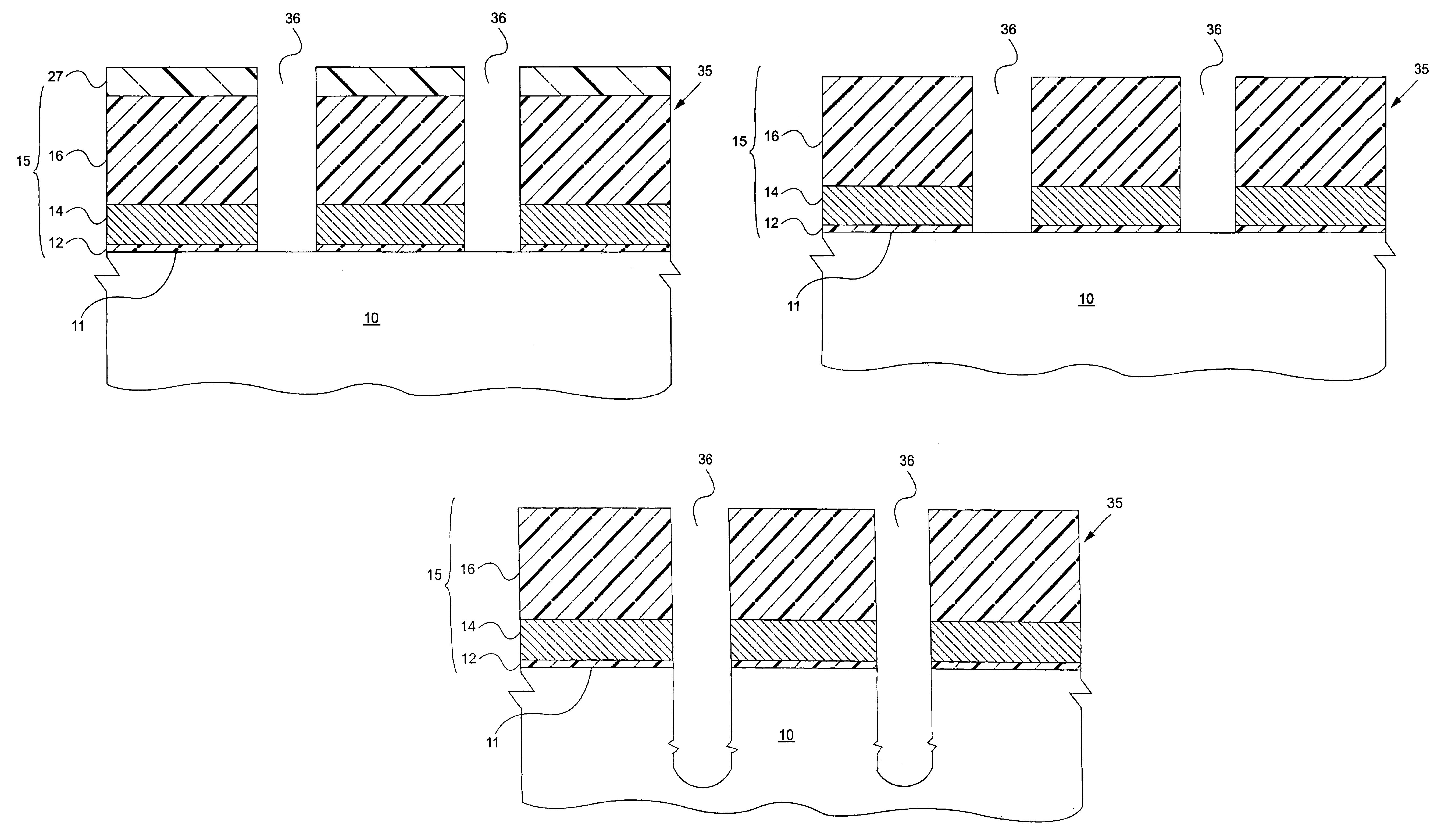
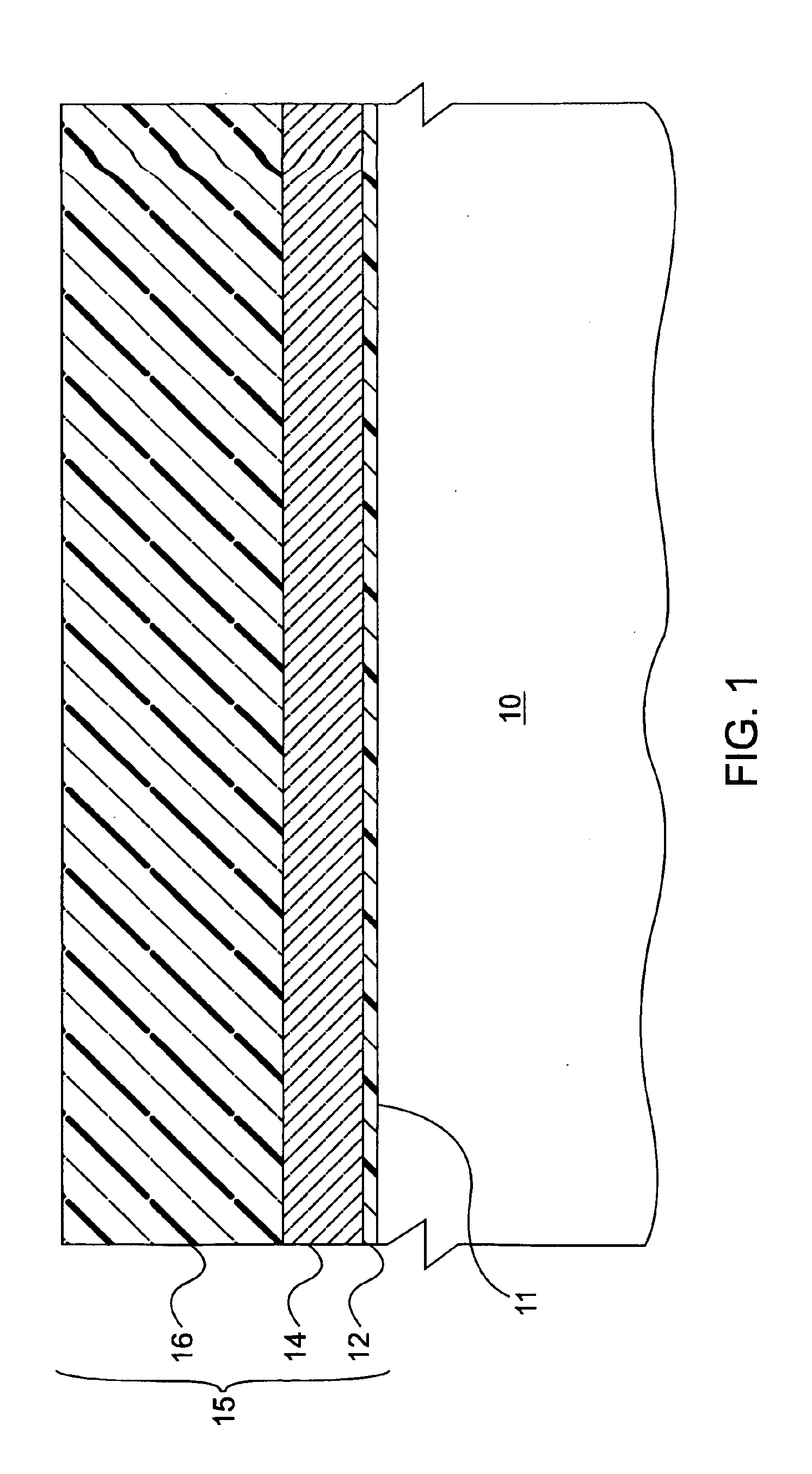
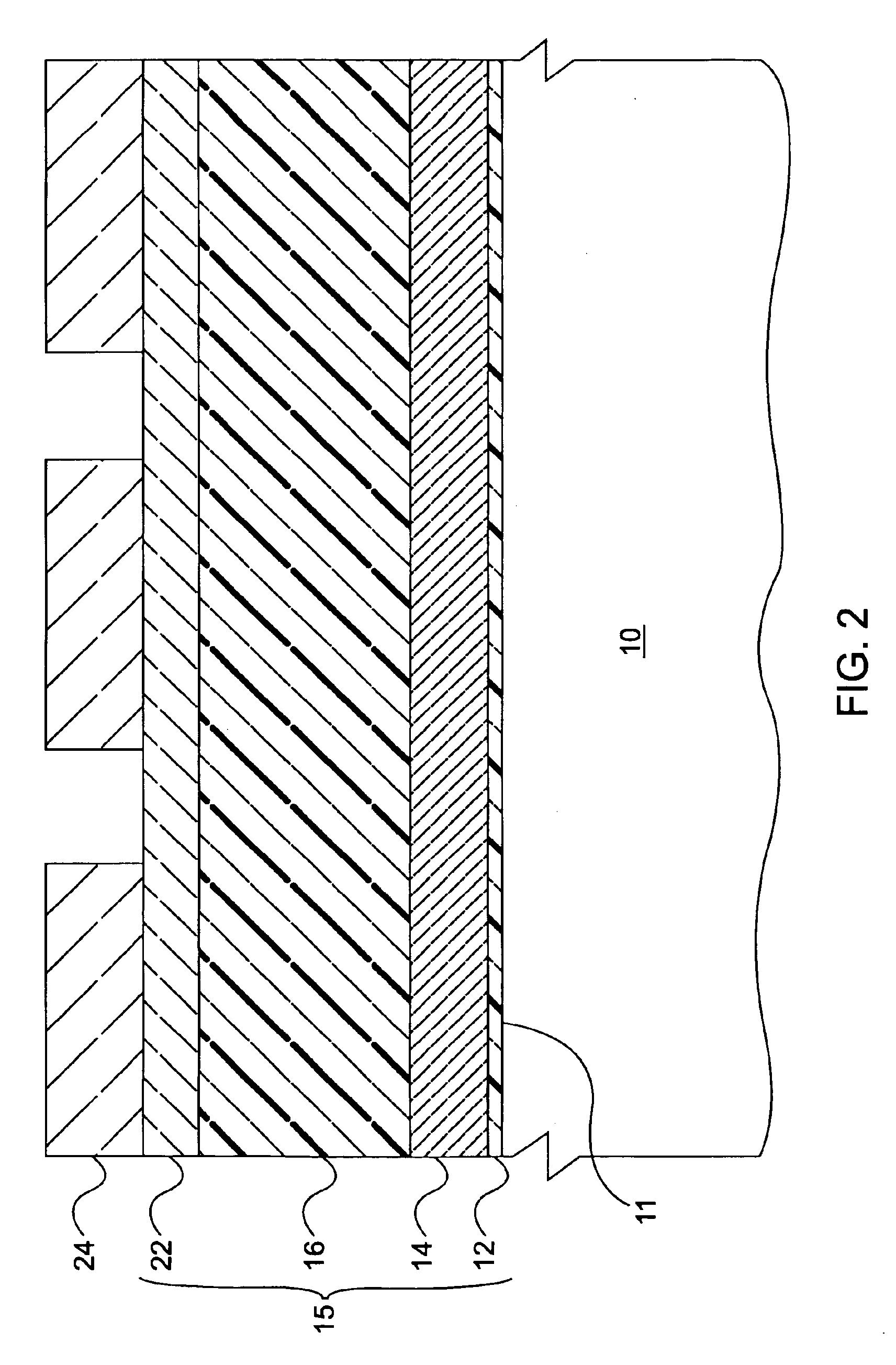
Generally, the present invention provides an etching process using a germanium hard mask. The germanium hard mask is formed by patterning a metallic germanium layer deposited over a dielectric layer disposed over a semiconductor substrate. Through the germanium hard mask, the dielectric layer is selectively etched to form a pattern over the semiconductor substrate, which is etched using the dielectric layer pattern as a mask. The patterning of the metallic germanium layer is preferably achieved using a thin mask, e.g., a thin photo resist mask. The germanium hard mask is stripped away through germanium oxidation and water rinse, both of which have minimum effects on the semiconductor substrate. In a preferred embodiment, the germanium hard mask is oxidized and rinsed away before etching the semiconductor substrate.

FIG. 1 is a schematic cross sectional view of a semiconductor substrate 10 at an early stage of an etching process in accordance with the present invention. Typically, sem...


PUM

PropertyMeasurementUnit
Thicknessaaaaaaaaaa
Thicknessaaaaaaaaaa
Thicknessaaaaaaaaaa

Abstract

An etching process using germanium hard mask (25) includes forming a dielectric layer (15) over a major surface (11) of a semiconductor substrate (10) and depositing a metallic germanium layer (22) over the dielectric layer (15). The metallic germanium layer (22) is patterned through a photo resist (24) to form the germanium hard mask (25). The dielectric layer (15) is selectively etched through the germanium hard mask (25) to form a dielectric hard mask (35), through which the semiconductor substrate (10) is subsequently etched. After forming the dielectric hard mask (35), the germanium hard mask (25) is stripped away by oxidizing the metallic germanium hard mask (25) to transform it into a layer (27) of germanium oxide and rinsing the semiconductor substrate (10) in water to remove the germanium oxide layer (27). Preferably, the germanium hard mask (25) is removed before etching the semiconductor substrate (10).

Description

FIELD OF THE INVENTIONThe present invention relates, in general, to semiconductor device fabrication and, more particularly, to etching processes used in the fabrication of semiconductor devices.BACKGROUND OF THE INVENTIONEtching is widely used in the fabrication of semiconductor devices. A process for etching a pattern, e.g., a trench, in a semiconductor substrate usually starts with forming a mask on the substrate. The substrate is then etched through the mask, which defines the pattern etched in the substrate. Photo resist is typically used for forming the mask. In some processes, e.g., deep trench etching, the etch selectivity to the photo resist material is insufficient, and the etching process depletes the photo resist mask and damages the underlying substrate.In such etching processes, a dielectric hard mask, e.g., a thick silicon dioxide or silicon nitride hard mask, can be used to effectively protect the underlying substrate. Patterning a thick dielectric hard mask requires...

Claims


Application Information

Patent Timeline
IPC IPC(8): H01L21/02H01L21/302C23F4/00C23G1/00H01L21/308H01L21/3213
CPCC23F4/00C23G1/00H01L21/32134H01L21/3086H01L21/3081
Inventor FURUKAWA, TOSHIHARUHAKEY, MARK C.HOLMES, STEVEN J.HORAK, DAVID V.MA, WILLIAM H-L.
Owner IBM CORP
Why Eureka
Try Eureka