
Highly transparent top electrode for OLED device

a top electrode, high-transmission technology, applied in the manufacture of electrode systems, cold cathode manufacturing, electric discharge tubes/lamps, etc., can solve the problems of reduced use life of oled devices, increased risk of operational degradation of display devices, and limited light emission area in the general area

Inactive Publication Date: 2005-04-05
GLOBAL OLED TECH
View PDF4 Cites 34 Cited by
  • Summary
  • Abstract
  • Description
  • Claims
  • Application Information

AI Technical Summary

Benefits of technology

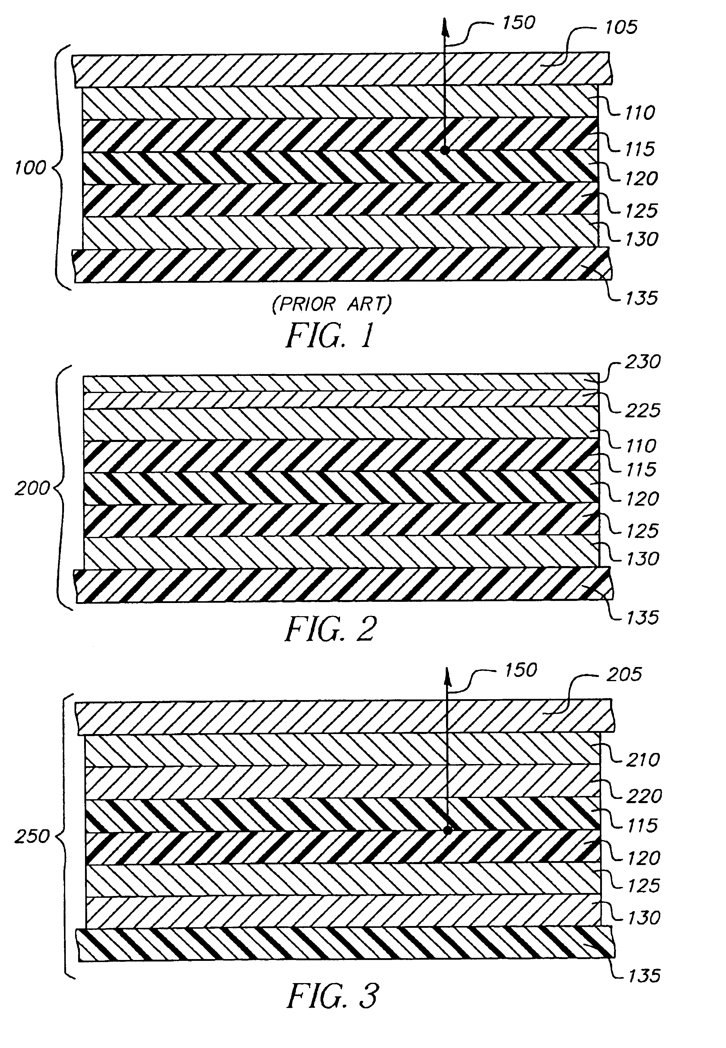
It is therefore an object of the present invention to provide an OLED device capable of emitting light through the top surface with high efficiency. It is a further object of this invention to enable manufacturing of OLEDs with a transparent cathode. It is a further object of this invention to optimize viewing and image quality in a TE OLED. It is a further object of this invention to provide protection for the organic layers during high-speed deposition of transparent cathode for the OLED.
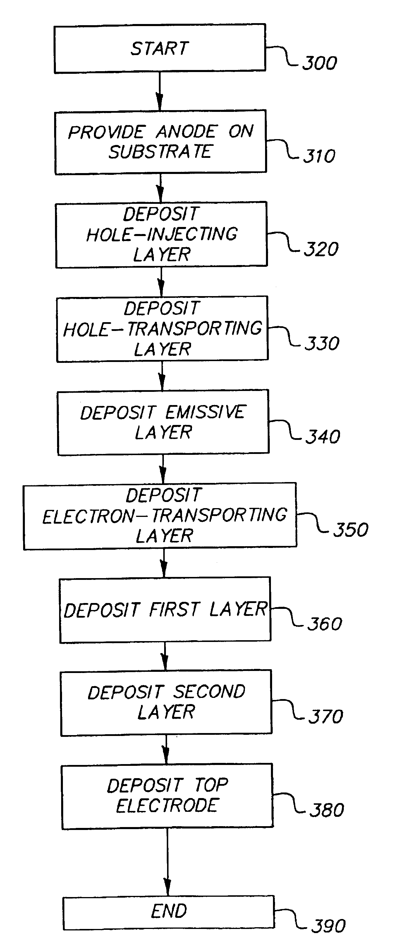
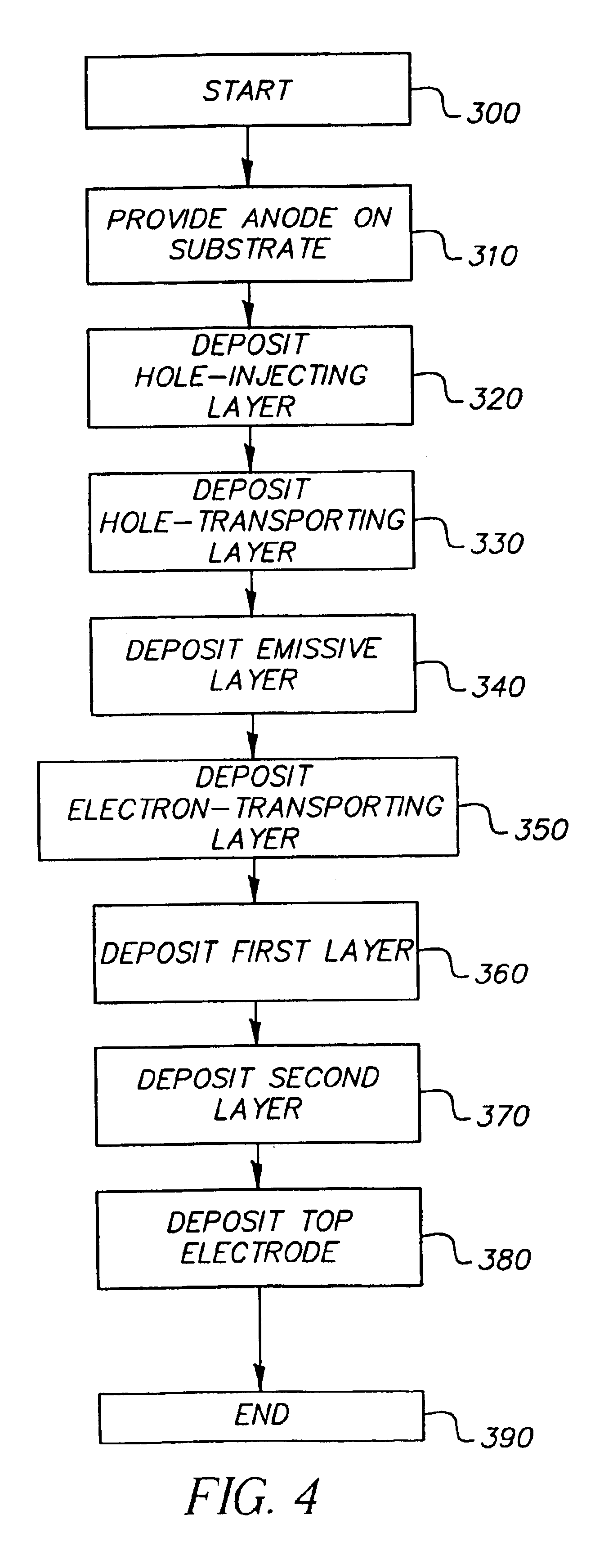
(c) providing first and second layers over the emissive layer with the first layer being in contact with the emissive layer and having a compound that includes an electron-injecting element, and the second layer having a reactive metal, and wherein such reactive metal reacts with the compound to release the electron-injecting element that dopes the interfacial region of the emissive layer to improve electron-injection and also reduces the reflectivity of the first and second layers is reduced; and
(e) providing first and second layers over the electron-transport layer with the first layer being in contact with the electron-transport layer and having a compound that includes an electron-injecting element, and the second layer having a reactive metal, and wherein such reactive metal reacts with the compound to release the electron-injecting element that dopes the interfacial region of the electron-transport layer to improve electron-injection and also reduces the reflectivity of the first and second layers is reduced; and
It is an advantage of the method of this invention that it enables manufacturing of top-emitting OLED devices in high volumes and at high speeds. It is a further advantage of this method that it reduces the microcavity effects and thereby produces an OLED with a wider range of viewing angles and with less color distortion.

Problems solved by technology

However, in this bottom-emitting type of display where light is emitted downward through the substrate, the overall area that can emit light is limited by the presence on the substrate of Thin Film Transistors (TFT's) and other circuitry, which are opaque.
To compensate for the reduced average brightness level, the drive current has to be increased subjecting the display to increased risk of operational degradation.
This results in the lower AR devices having a shorter useable life than a device with a higher AR.
These metallic materials contribute to a microcavity effect within the devices that limits the optical qualities.
Highly transparent materials (e.g., indium-tin-oxide (ITO)) are being considered to replace the semi-reflective cathodes; however, known deposition methods for these materials are not compatible with the said structure designs, and these highly transparent materials are less electrically conductive than the semi-reflective materials.
The fact that these materials are less electrically conductive makes implementing a highly transparent cathode in a large display difficult because of the greater distance that the current must travel.
This solution for delivering a highly transparent cathode for use in an OLED is insufficient because it: 1) does not optimize the electron injection into the electron transport layer; and 2) uses materials unsuitable for full color devices.
Destructive light interference can result from micro-cavity effects within a top-emitting OLED with a reflective cathode and can cause color distortion when the top-emitting OLED is viewed from oblique angles.
However, sputtering can be damaging to the electron transport layer (ETL) within OLED devices.
This damage reduces the intensity of the emission and may additionally render the pixels permanently inoperable.

Method used


Image

  • Highly transparent top electrode for OLED device
  • Highly transparent top electrode for OLED device
  • Highly transparent top electrode for OLED device

Examples


example 1

A prior-art bottom-emitting device, device “1A”, was made as described above with 1% C545T as the emissive layer dopant. The device has the following layer structure:Glass(1.1 mm) / ITO(42 nm) / CFx(1 nm) / NPB(50 nm) / 1% C545T in Alq (30 nm) / Alq(20 nm) / LiF(0.5 nm) / Al(100 nm)

example 2

A top-emitting device of the present invention, device “2B” was made with the same hole-transporting, emissive, and electron-transporting layers as the device “1A”. The device “2B” has the following layer structure:Glass(1.1 mm) / Ag(100 nm) / CFx(1 nm) / NPB(50 nm) / 1% C545T in Alq (30 nm) / Alq(20 nm) / RbF(3 nm) / Mg(5 nm) / ITO(60 nm)

example 3

A prior-art bottom-emitting device, device “3A”, was made as described above with 1% DCJTB as the emissive layer dopant. The device has the following layer structure:Glass(1.1 mm) / ITO(42 nm) / CFx(1 nm) / NPB(60 nm) / 1% DCJTB in Alq (30 nm) / Alq(30 nm) / LiF(0.5 nm) / Al(70 nm)


PUM

PropertyMeasurementUnit
Thicknessaaaaaaaaaa
Currentaaaaaaaaaa
Thicknessaaaaaaaaaa

Abstract

A method of making an OLED device capable of emitting light through the top electrode of such device includes providing a substrate and an anode over the substrate; providing an emissive layer disposed over the anode; providing first and second layers over the emissive layer with the first layer being in contact with the emissive layer or electron-transport layer and having a compound that includes an electron-injecting element, and the second layer having a reactive metal, and wherein such reactive metal reacts with the compound to release the electron-injecting element that dopes the interfacial region of the emissive layer or electron-transport layer to improve electron-injection and also reduces the reflectivity of the first and second layers is reduced; and providing a transparent conducting non-metallic top electrode over the second layer.

Description

FIELD OF THE INVENTIONThe present invention relates to OLED devices having a highly transmissive top electrode.BACKGROUND OF THE INVENTIONOrganic electroluminescent displays, commonly called OLED devices for organic light-emitting diode devices, are typically coupled with active matrix (AM) circuitry in order to produce high performance displays. The basic OLED device has in common an anode, a cathode, and an organic electroluminescent medium sandwiched between the anode and the cathode. Such a display is disclosed in U.S. Pat. No. 5,550,066. However, in this bottom-emitting type of display where light is emitted downward through the substrate, the overall area that can emit light is limited by the presence on the substrate of Thin Film Transistors (TFT's) and other circuitry, which are opaque. Consequently the open area available for the light to emerge is reduced. The ratio of open area to that of the entire device area is called the Aperture Ratio (AR). Due to the reduction of th...

Claims


Application Information

Patent Timeline
IPC IPC(8): H01L51/52H01L51/50H05B33/10H05B33/28
CPCH01L51/5092H01L51/5221H01L2251/5315H10K50/171H10K2102/3026H10K59/8052H05B33/10H10K50/82
Inventor RAYCHAUDHURI, PRANAB K.MADATHIL, JOSEPH K.
Owner GLOBAL OLED TECH
Learn More