Semiconductor device having a trench isolation and method of fabricating the same

a semiconductor device and trench isolation technology, applied in the field of semiconductor devices, can solve the problems of deterioration of operation breakdown voltage resistance, frequency dependence of delay time, heat treatment after implanting impurities, etc., and achieve the effect of preventing deterioration of transistor characteristics

Inactive Publication Date: 2005-04-05
RENESAS ELECTRONICS CORP
View PDF34 Cites 29 Cited by
  • Summary
  • Abstract
  • Description
  • Claims
  • Application Information

AI Technical Summary

Benefits of technology

An object of the present invention is to provide a method of fabricating a semiconductor device in which deterioration in a transistor characteristic is prevented by preventing a channel stop implantation layer from being formed in an active region.

Problems solved by technology

Consequently, there is a tendency that heat treatment after implanting impurities is performed at low temperature in short time.
However, there are various problems caused by a substrate floating effect, such as accumulation of carriers (holes in the NMOS) generated by an impact ionization in the channel forming region, occurrence of a kink due to the accumulated carriers, deterioration in operation breakdown voltage resistance, and occurrence of frequency dependency of delay time caused by an unstable potential of the channel forming region.
However, there is a case that, in the well region under the partial isolation oxide film, the impurity concentration decreases due to a segration phenomenon at the time of forming an oxide film, and the conduction type reverses.
Consequently, even if the channel stop implantation is performed before the trench isolation structure is formed, there is the possibility that the impurities are diffused in the heat treatment performed after that, the profile is disturbed, and an intended effect cannot be obtained.
However, in this case, a problem arises such that it is difficult to implant impurities of high concentration into only the region under the trench isolation oxide film.
As a result, it becomes difficult to adjust the threshold value of a MOS transistor and to make the source / drain layer of the MOS transistor or a depletion layer formed around a PN junction of the source / drain layer reach buried oxide film 102.

Method used


Image

  • Semiconductor device having a trench isolation and method of fabricating the same
  • Semiconductor device having a trench isolation and method of fabricating the same
  • Semiconductor device having a trench isolation and method of fabricating the same

Examples


first embodiment

A. First Embodiment

A-1. Fabricating Method

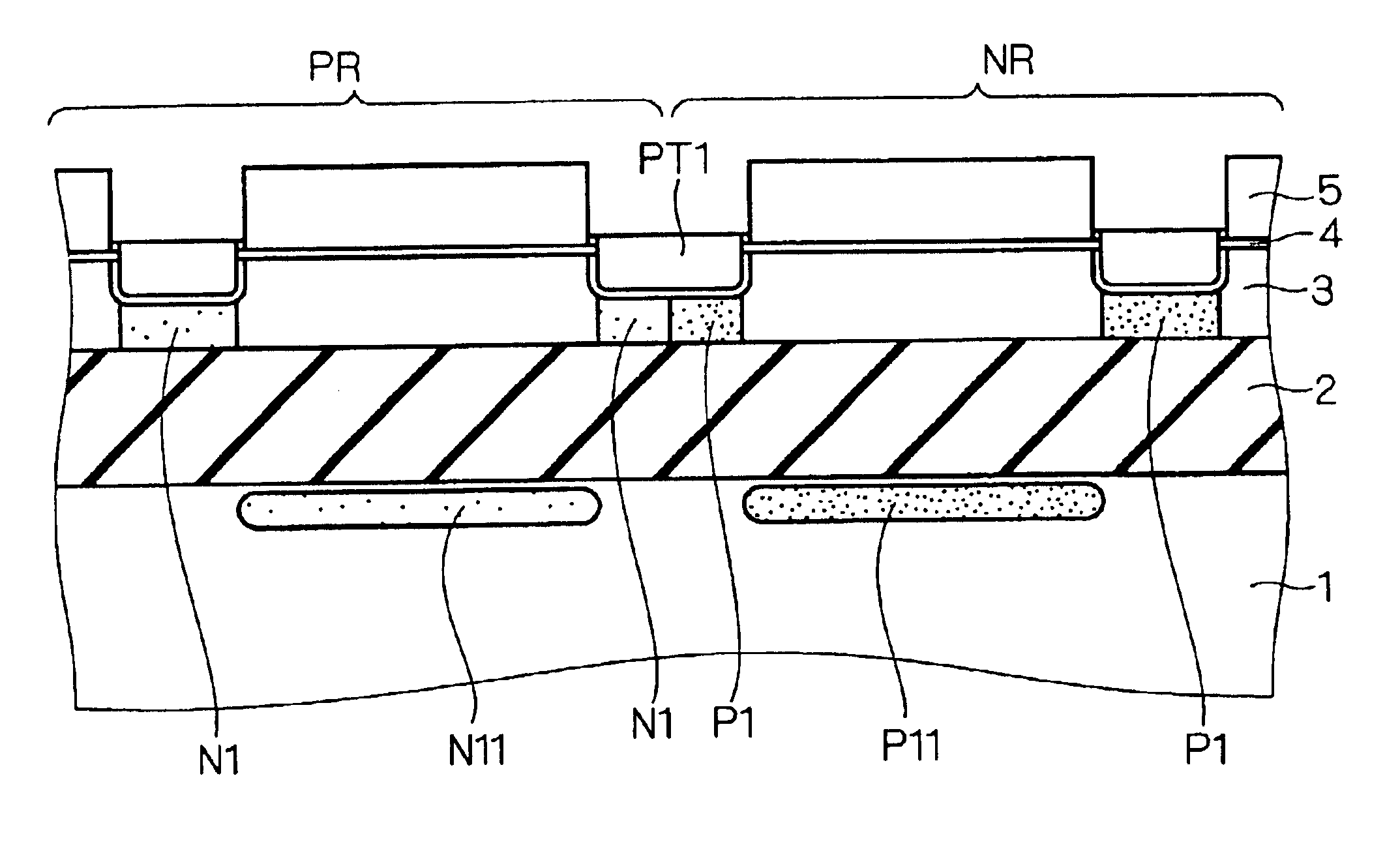
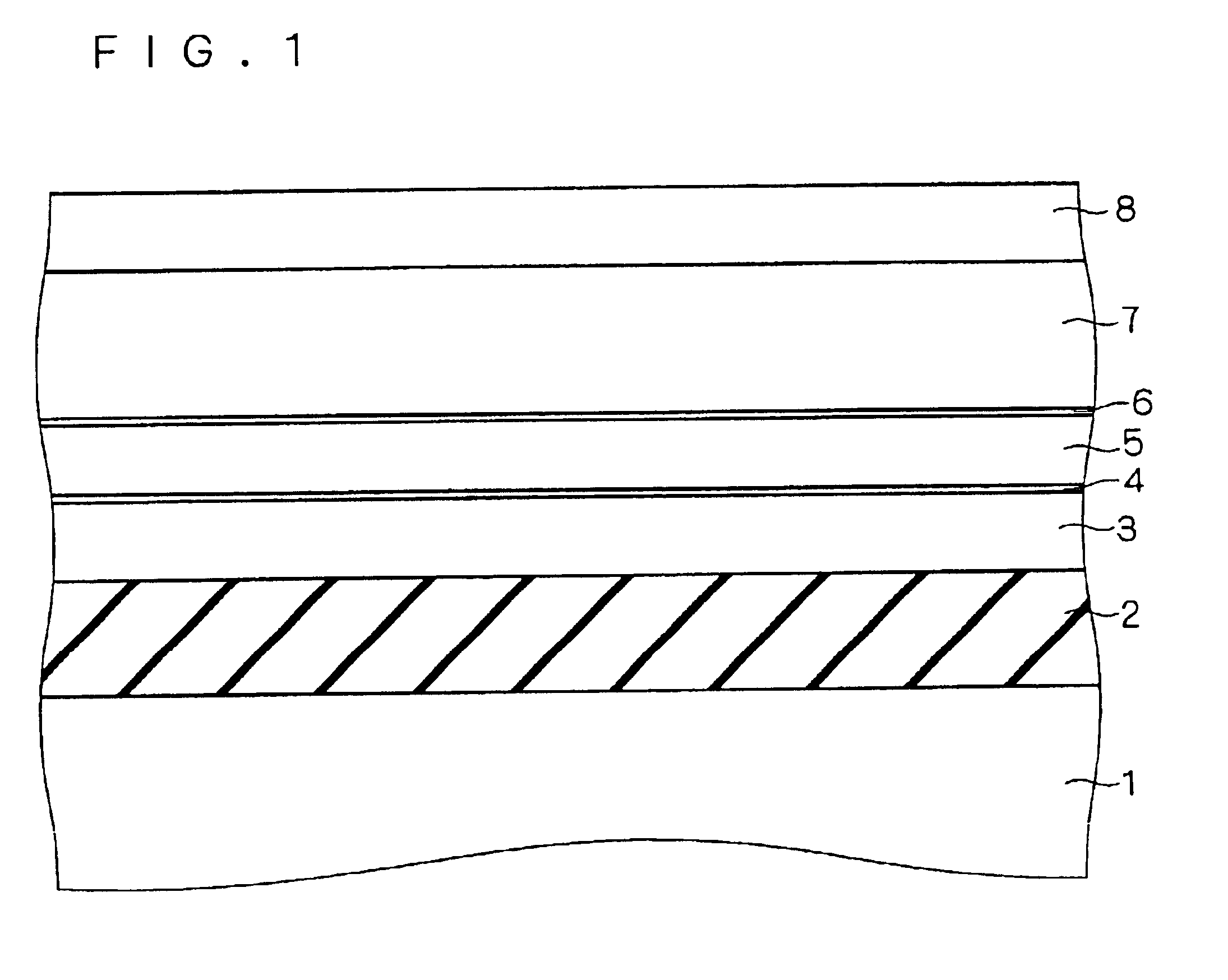
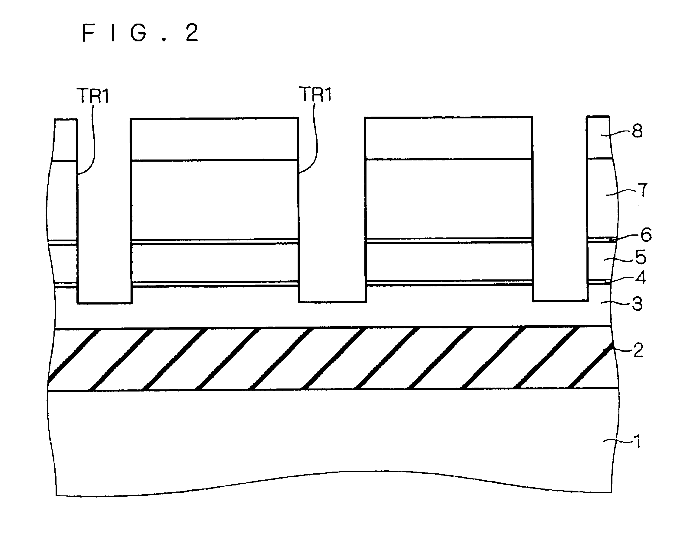
With reference to FIGS. 1 to 13 as cross sections for sequentially showing a fabricating process, a fabricating method of a first embodiment according to the present invention will be described.

First, as shown in FIG. 1, by the SIMOX method for forming a buried oxide film 2 by oxygen ion implantation, bonding, or the like, an SOI substrate constructed by a silicon substrate 1, a buried oxide film 2, and an SOI layer 3 is prepared. The SOI substrate may be formed by a method other than the above methods.

Usually, the film thickness of SOI layer 3 is 50 to 200 nm, and the film thickness of buried oxide film 2 is 100 to 500 nm. On the SOI substrate, a silicon oxide film (hereinafter, called an oxide film) 4 having a thickness of 10 to 30 nm (100 to 300 Å) is formed by CVD (with a temperature condition of about 800° C.) or thermal oxidation (with a temperature condition of 800 to 1000° C.).

After that, a polycrystalline silicon film (hereinbelow, ...

second embodiment

B. Second Embodiment

Although the configuration of performing the channel stop implantation through the partial isolation oxide film having a large isolation step is used in the first embodiment, channel stop implantation may be also performed by a method described hereinbelow.

B-1. Fabricating Method

With reference to FIGS. 14 to 20 as cross sections for sequentially showing a fabricating process, a fabricating method of a second embodiment according to the present invention will be described. The same components as those in the first embodiment described by referring to FIGS. 1 to 13 are designated by the same reference numerals and their description will not be repeated.

First, as shown in FIG. 14, oxide film 4 is formed on an SOI substrate.

A polysilicon film 21 having a thickness of 5 to 300 nm (50 to 3000 Å) is formed on oxide film 4 by CVD. A nitride film 22 having a thickness of 100 to 200 (1000 to 2000 Å) is formed on polysilicon film 21 by CVD. Oxide film 4, polysilicon film 21...

third embodiment

C. Third Embodiment

In the second embodiment, the configuration of performing channel stop implantation in a state where polysilicon film 21 and nitride film 22 are left on active region AR has been described. The channel stop implantation may be also carried out by a method described hereinbelow.

C-1. Fabricating Method

With reference to FIGS. 22 to 27 as cross sections for sequentially showing a fabricating process, a fabricating method of a third embodiment according to the present invention will be described. The same components as those in the first and second embodiments described by referring to FIGS. 1 to 13 and FIGS. 14 to 20 are designated by the same reference numerals and their description will not be repeated.

First, by performing the processes described with reference to FIGS. 14 to 17, oxide film OX2 in trench TR2 and removing oxide film OX2 on nitride film 22 and nitride film 22 by CMP. As shown in FIG. 22, the main surface of polysilicon film 21 can be exposed.

After tha...


PUM


Abstract

The present invention provides a method of fabricating a semiconductor device in which deterioration in a transistor characteristic is prevented by preventing a channel stop implantation layer from being formed in an active region. A resist mask is formed so as to have an opening over a region in which a PMOS transistor is formed. Channel stop implantation is performed with energy by which ions pass through a partial isolation oxide film and a peak of an impurity profile is generated in an SOI layer, thereby forming a channel stop layer in the SOI layer under the partial isolation oxide film, that is, an isolation region. An impurity to be implanted here is an N-type impurity. In the case of using phosphorus, its implantation energy is set to, for example, 60 to 120 keV, and the density of the channel stop layer is set to 1×10¹⁷ to 1×10¹⁹/cm3. At this time, the impurity of channel stop implantation is not stopped in the SOI layer corresponding to the active region.

Description

BACKGROUND OF THE INVENTION1. Field of the InventionThe present invention relates to a semiconductor device and, more particularly, to a method of fabricating a semiconductor device having a trench isolation oxide film.2. Related Background ArtA semiconductor device of an SOI (Silicon On Insulator) structure (hereinbelow, called an SOI device) formed on an SOI substrate in which a buried oxide film and an SOI layer are formed on a silicon substrate has characteristics such as reduced parasite capacity, high-speed operation, and low power consumption and is used for a portable device and the like.Also for a bulk device directly formed on a silicon substrate, microfabrication technology and high integration technique progress conspicuously, and the speed of development of the bulk device is increasing.In association with a progress of a device technique, the concentration of a channel impurity and that of a source / drain impurity are getting higher and, moreover, a sharp impurity profi...

Claims


Application Information

Patent Timeline
Patent Type & Authority Patents(United States)
IPC IPC(8): H01L21/762H01L21/70H01L27/12H01L21/84H01L21/336H01L21/76H01L27/08H01L29/786
CPCH01L21/2652H01L21/76264H01L27/1203H01L21/84H01L21/76283H01L21/76
Inventor IWAMATSU, TOSHIAKIIPPOSHI, TAKASHIMATSUMOTO, TAKUJIMAEDA, SHIGENOBU
Owner RENESAS ELECTRONICS CORP
Why Eureka
Try Eureka