Semiconductor memory device

a memory device and semiconductor technology, applied in semiconductor devices, digital storage, instruments, etc., can solve the problems of increasing the power consumption of the whole chip, the inability to make fast read rates, and the increase of the current consumption so as to reduce the leakage current of the memory cell, the operating speed of the peripheral circuit can be made fast, and the power consumption can be reduced

a memory device and semiconductor technology, applied in semiconductor devices, digital storage, instruments, etc., can solve the problems of increasing the power consumption of the whole chip, the inability to make fast read rates, and the increase of the current consumption so as to reduce the leakage current of the memory cell, the operating speed of the peripheral circuit can be made fast, and the power consumption can be reduced

US6876573B2Inactive Publication Date: 2005-04-05HITACHI LTD

Image

  • Semiconductor memory device
  • Semiconductor memory device
  • Semiconductor memory device

Examples


first embodiment

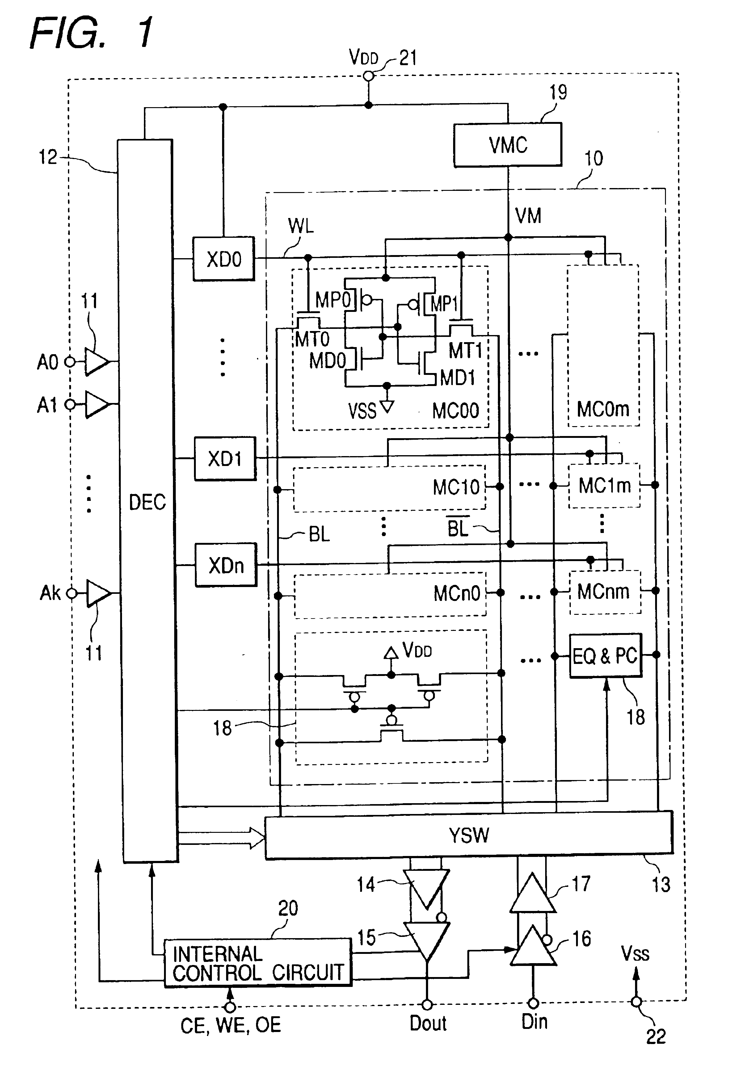
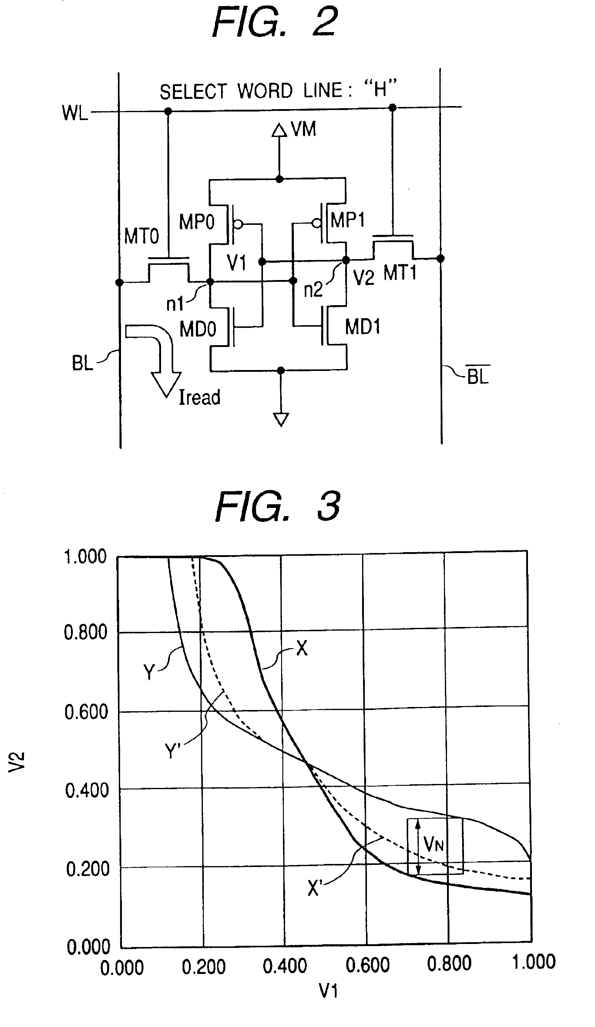
[0039]In the first embodiment, a booster or step-up circuit 19 for boosting the source or power supply voltage VDD like 0.6V supplied to the power supply terminal 21 from outside and generating a boost voltage VM like, e.g., 1.2V is provided. Along with it, the boost voltage VM generated by the step-up circuit 19 is applied to a source or power-supply voltage terminal of the memory array 10, i.e., source terminals of P-MOSs MP0 and MP1 of each memory cell MC as an operating voltage. Incidentally, a ground potential VSS is applied to source terminals of N-MOSs MD0 and MD1 of each memory cell MC.

[0040]On the other hand, the external power supply voltage VDD is applied to source or power-supply voltage terminals of peripheral circuits such as the address decoder 12 and word drivers XD0 through XDn except for the memory array 10 as an operating voltage. Except for at standby, i.e., upon read and write, all the word lines WL in the memory array 10 are respectively brought to a low level ...

second embodiment

[0056]Further, gate insulating films for the MOSFETs MT0, MT1; MP0 and MP1; and MD0 and MD1 constituting the memory cell MC, and high voltage-applied MOSFETs (P-MOSs) of MOSFETs constituting the word drivers XD0 through XDn are formed so as to become thicker than a gate insulating film for MOSFETs constituting other peripheral circuits such as a decoder circuit 12 in the Thus, even if the boost voltage VM is applied to source terminals of these MOSFETs, such a withstand voltage as not to degrade the gate insulating film is given.

[0057]FIG. 7 shows parts of the decoder circuit 12 and the word drivers XD0 through XDn. DEC indicates a unit decoder comprising NAND gates with internal address signals ai and ai+1 as input signals, and INV indicates an inverter for inverting an output thereof. Although not restricted in particular in the second embodiment, word lines are respectively formed as hierarchical configurations each of which comprises a main word line MWL and a plurality of sub ...


PUM


Abstract

A semiconductor memory device having a memory array comprising CMOS flip-flop circuit type memory cells, which is capable of improving a noise margin, making a read rate fast and reducing power consumption. In the semiconductor memory device, an operating voltage of the memory cell is set higher than an operating voltage of each of peripheral circuits. Threshold voltages of MOS transistors that constitute the memory cell, are set higher than those of MOS transistors constituting the peripheral circuit. A gate insulting film for the MOS transistors that constitute the memory cell, is formed so as to be regarded as thicker than a gate insulting film for the MOS transistors constituting the peripheral circuit when converted to an insulating film of the same material. Further, a word-line selection level and a bit-line precharge level are set identical to the level of the operating voltage of the peripheral circuit.

Description

[0002]This application is a Divisional of U.S. Ser. No 10 / 671,475 filed Sep. 29, 2003 now U.S. Pat. No. 6,791,895, issued on Sep. 14, 2004 which is a Divisional of U.S. Ser. No. 10 / 198,925 filed Jul. 22, 2002 now U.S. Pat. No. 6,657,887. Priority is claimed based on U.S. Ser. No. 10 / 671,475 filed Sep. 29, 2003 which claims priority to U.S. Ser. No. 10 / 198,925 filed Jul. 22, 2002, which claims priority to Japanese Patent Application No. 2001-241594 filed on Aug. 9, 2001.BACKGROUND OF THE INVENTION[0003]The present invention relates to a semiconductor memory device and a technology for improving a noise margin and an operating speed of an SRAM (Static Random Access Memory) and achieving low power consumption thereof, e.g., a technology effective for application to an SRAM having CMOS flip-flop circuit type memory cells or an LSI (Large Scale Integration) with the SRAM built therein.[0004]In a semiconductor memory device (hereinafter called a “semiconductor memory” or simply “memory”) ...

Claims


Application Information

Patent Timeline
05 Apr 2005
Publication
US6876573B2
IPC
G11C11/412; G11C11/417; G11C8/02; G11C11/41; G11C11/413; H01L27/10; H10B10/00
CPC
G11C11/417; G11C11/412; H10B10/00
Inventors
HIGETA, KEIICHI; NAKAHARA, SHIGERU