Thin film magnetic memory device having a magnetic tunnel junction

Inactive Publication Date: 2005-04-05
RENESAS ELECTRONICS CORP
View PDF13 Cites 34 Cited by
  • Summary
  • Abstract
  • Description
  • Claims
  • Application Information

AI Technical Summary

Benefits of technology

Accordingly, a primary advantage of the present invention is the ability to change a voltage on the source lines between the precharging operation and the data read operation. This prevents an unnecessary charging/discharging current from flowing through the first data lines that do not directly relate to the data read operation, allowing for reduction in power consumption in the data read operation.
A thin film magnetic memory device according to another aspect of the present invention includes memory cell, a first signal line and a second signal line. The memory cell is provided in order to store data, and includes a magnetic storage portion having its electric resistance value varying according to a storage data level. The magnetic storage portion includes a first magnetic layer retaining a prescribed fixed magnetization direction, and a second magnetic layer retaining a magnetization direction written according to combination of a first data write magnetic field for applying a magnetic field in a hard magnetization direction and a second data write magnetic field for applying a magnetic field in an easy magnetization direction. The first signal line passes therethrough a first data write current generating the first data write magnetic field. The second signal line passes therethrough a second data write current generating the second data write magnetic field. In data write operation, supply of the first data write current is started prior to supply of the second data write current.
Thus, in the data write operation to the magnetic storage portion, the magnetic field in the easy axis direction is generated after generation of the magnetic field in the hard axis direction, thereby enabling stable data write operation in view of the magnetic characteristics of the memory cell.
A thin film magnetic memory device according to still another aspect of the present invention includes a plurality of memory cells, a plurality of write word lines, a plurality of bit lines, a plurality of source lines, and a plurality of coupling switch data write circuits. The plurality of memory cells are arranged in a matrix. Each of the plurality of memory cells includes a magnetic storage portion having its electric resistance value varying according to a storage data level written therein by combination of first and second data write magnetic fields. The plurality of write word lines are provided respectively corresponding to memory cell rows, and are selectively activated in data write operation to pass therethrough a first data write current for generating the first data write magnetic field. The plurality of bit lines are provided respectively corresponding to memory cell columns. The plurality of source lines are provided respectively corresponding to the memory cell columns. Each of the plurality of source lines interposes the memory cells on a corresponding memory cell column between

Problems solved by technology

Therefore, a wasteful charging/discharging current that does not directly contribute to the data read operation is produced in the bit lines of the non-selected memory cell columns (hereinafter, also simply referred to as “non-selected columns”), thereby increasing the power consumption in the data read operation.
This may possibly hinder the speed and stability of the data read op

Method used


Image

  • Thin film magnetic memory device having a magnetic tunnel junction
  • Thin film magnetic memory device having a magnetic tunnel junction
  • Thin film magnetic memory device having a magnetic tunnel junction

Examples


first embodiment

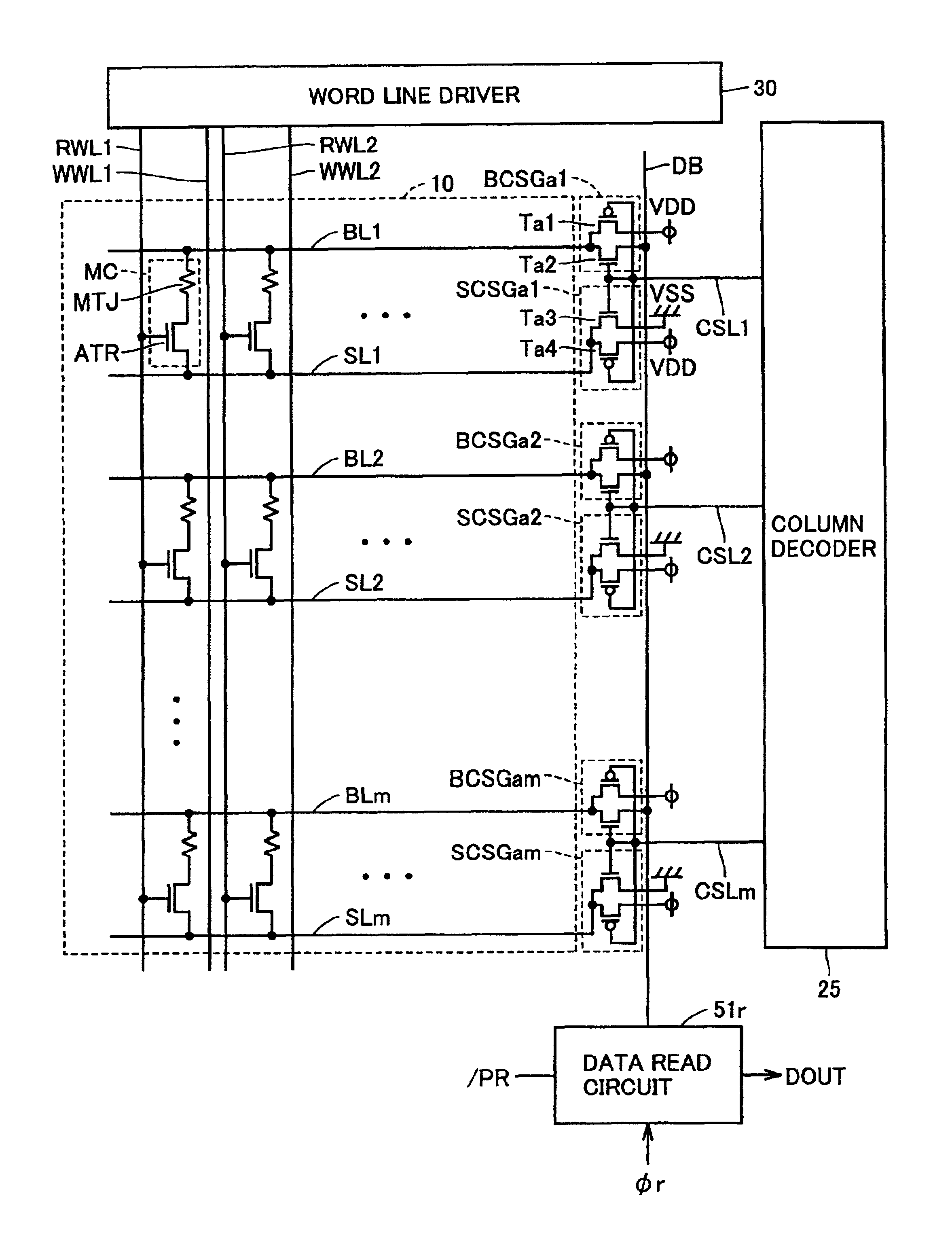
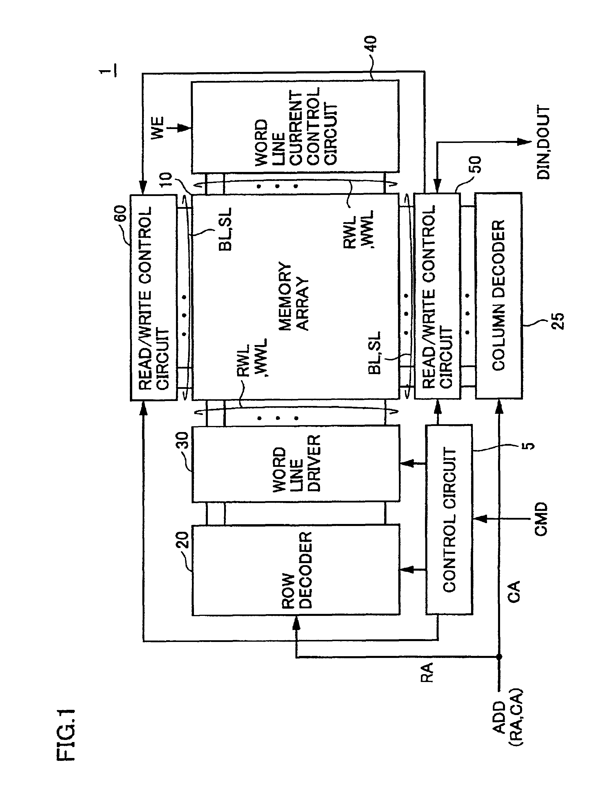
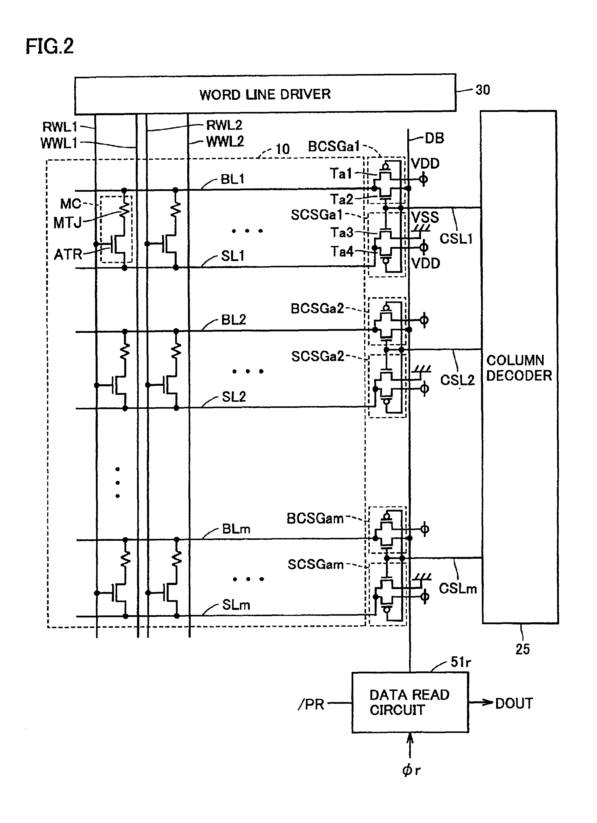
Referring to FIG. 1, an MRAM device 1 according to a first embodiment of the present invention conducts random access in response to an external control signal CMD and address signal ADD, thereby receiving write data DIN and outputting read data DOUT.

The MRAM device 1 includes a control circuit 5 for controlling the overall operation of the MRAM device 1 in response to the control signal CMD, and a memory array 10 having a plurality of MTJ memory cells arranged in a matrix. Although the structure of the memory array 10 will be specifically described below, a plurality of write word lines WWW and a plurality of read word lines RWL are provided respectively corresponding to the MTJ memory cell rows. Bit lines BL and source lines SL are provided respectively corresponding to the MTJ memory cell columns.

The MRAM device 1 further includes a row decoder 20, a column decoder 25, a word line driver 30, a word line current control circuit 40 and read / write control circuits 50, 60.

The row dec...

second embodiment

The structure for supplying a data write current so as to stabilize the data write operation to the memory cell will be described in the second embodiment.

Referring to FIG. 15, in the second embodiment, the memory cells MC, read word lines RWL, bit line pairs BLP, source lines SL and the like in the memory array 10, and the circuitry associated with the data read operation have the same structure as that of FIG. 13. Therefore, detailed description thereof will not be repeated.

FIG. 15 additionally shows a word line current control circuit 40 for supplying a data write current, and a data write circuit 51w. Bit line coupling transistors 62 are provided respectively corresponding to the bit line pairs. The bit line coupling transistors 62 are provided in the region located opposite to the bit line selection gates BCGSb and the source line selection gates SCSGb with the memory array 10 interposed therebetween. FIG. 15 exemplarily shows a bit line coupling transistor 62-1 corresponding t...

third embodiment

The structure for efficiently supplying a data write current is described in the third embodiment.

Referring to FIG. 25, in the structure of the third embodiment, a memory array 10 includes memory cells MC arranged in n rows by m columns. In the memory array 10, read word lines RWL1, RWL2, . . . and write word lines WWL1, WWL2, are provided respectively corresponding to the memory cell rows. Bit lines BL1 to BLm and source lines SL1 to SLm are provided respectively corresponding to the memory cell columns.

The word line current control circuit 40 couples each write word line WWL to the ground voltage VSS in the region located opposite to the word line driver 30 with the memory array 10 interposed therebetween.

A data bus pair DBP of data buses DB, / DB is provided in a region adjacent to the memory array 10 so as to extend in the same direction as that of the read word lines RWL and the write word lines WWL.

Column selection lines CSL1 to CSLm, write column selection lines WCSL1 to WCSLm...


PUM


Abstract

Bit lines and source lines are precharged to a power supply voltage before data read operation. In the data read operation, a corresponding bit line is coupled to a data bus as well as a corresponding source line is driven to a ground voltage only in the selected memory cell column. In the non-selected memory cell columns, the bit lines and the source lines are retained at the precharge voltage, i.e., the power supply voltage. No charging/discharging current is produced in the bit lines of the non-selected memory cell columns, that is, a charging/discharging current that does not directly contribute the data read operation is not produced, thereby allowing for reduction in power consumption in the data read operation.

Description

BACKGROUND OF THE INVENTION1. Field of the InventionThe present invention generally relates to a thin film magnetic memory device. More particularly, the present invention relates to a thin film magnetic memory device capable of random access and including memory cells having a magnetic tunnel junction (MTJ).2. Description of the Background ArtAn MRAM (Magnetic Random Access Memory) device has attracted attention as a memory device capable of non-volatile data storage with low power consumption. The MRAM device is a memory device capable of non-volatile data storage using a plurality of thin film magnetic elements formed in a semiconductor integrated circuit and also capable of random access to each thin film magnetic element.In particular, recent announcement shows that the performance of the MRAM device is significantly improved by using tunnel magnetic resistive elements having a magnetic tunnel junction (MTJ) as memory cells. The MRAM device including memory cells having a magne...

Claims


Application Information

Patent Timeline
IPC IPC(8): G11C11/15G11C11/02G11C11/14
CPCG11C11/15
Inventor HIDAKA, HIDETO
Owner RENESAS ELECTRONICS CORP
Why Eureka
Try Eureka