Method for fabricating a non-volatile memory and metal interconnect process

a metal interconnect and non-volatile technology, applied in the direction of semiconductor devices, electrical equipment, basic electric elements, etc., can solve the problems of affecting the reliability of the memory device, clustering of charges on the surface of the insulator layer, etc., and achieve the effect of preventing a wide threshold voltage distribution

Active Publication Date: 2005-04-19
MACRONIX INT CO LTD
View PDF5 Cites 11 Cited by
  • Summary
  • Abstract
  • Description
  • Claims
  • Application Information

AI Technical Summary

Benefits of technology

[0012]An object of the present invention is to provide a method for fabricating a non-volatile memory, wher...

Problems solved by technology

However, if defects are present in the tunneling oxide layer underneath the polysilicon floating gate, current leakage easily occurs, which affects th...

Method used


Image

  • Method for fabricating a non-volatile memory and metal interconnect process
  • Method for fabricating a non-volatile memory and metal interconnect process
  • Method for fabricating a non-volatile memory and metal interconnect process

Examples


Embodiment Construction

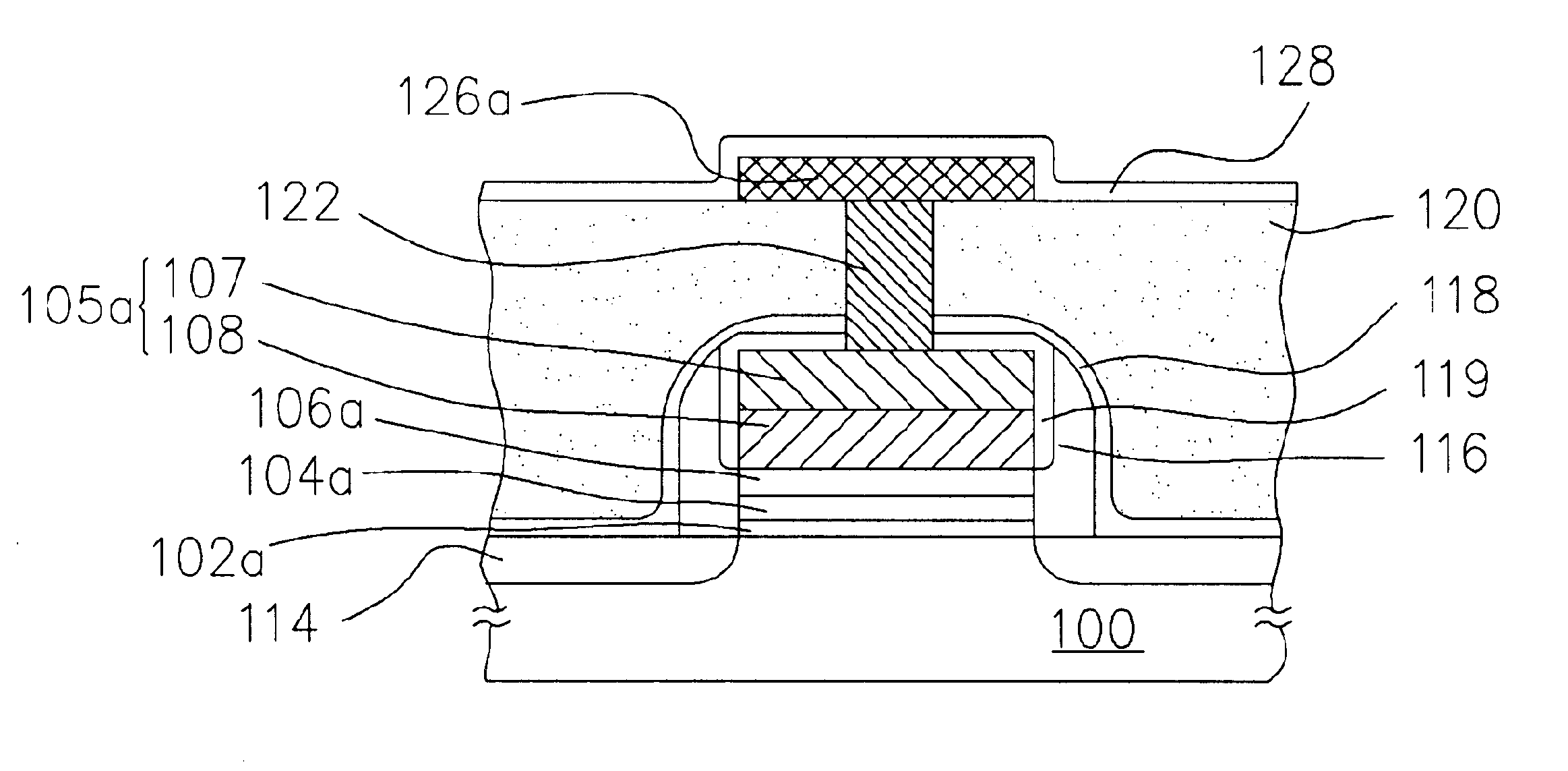
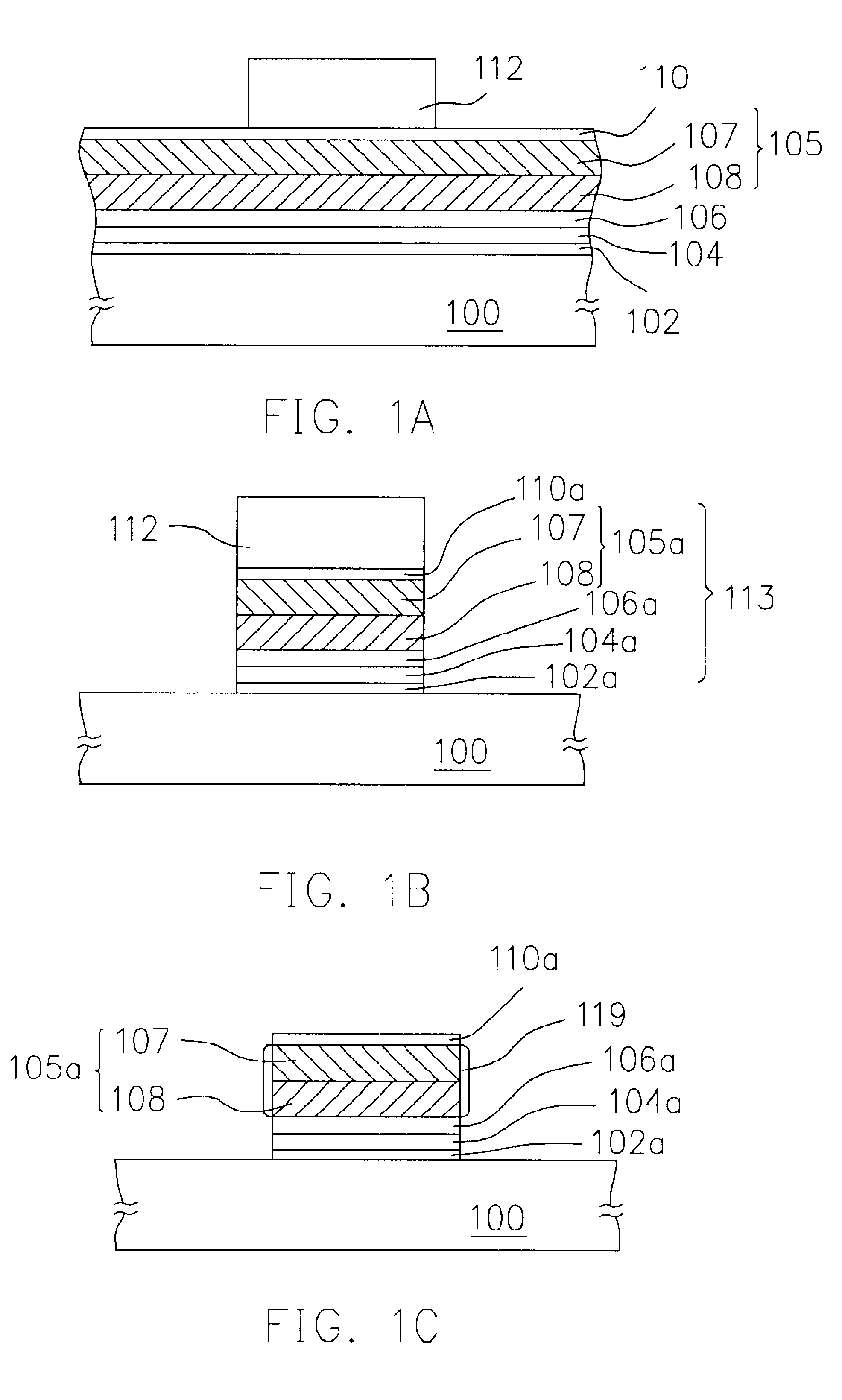
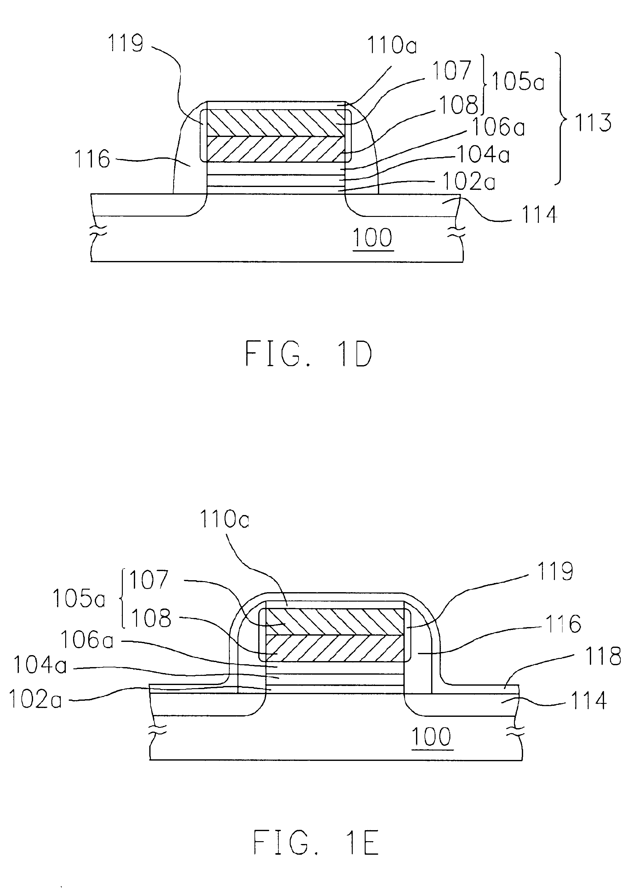
[0025]FIGS. 1A-1G are cross-sectional views showing the progression of steps for fabricating a non-volatile memory in accordance with an embodiment of the present invention. Referring to FIG. 1A, a tunneling layer 102, a trapping layer 104 and barrier layer 106 are sequentially formed on a substrate 102. The material of the substrate 100 is, for example, silicon; the barrier layer 102 is, for example, a silicon oxide layer. The trapping layer 104 is, for example, a silicon nitride layer. The barrier layer 106 is, for example, a silicon oxide layer.

[0026]A polysilicon layer 108 and a metal silicide layer 107 are sequentially formed on the barrier layer 106, wherein the polysilicon layer 108 and the metal silicide layer 107 form a gate conductive layer 105. An anti-reflection layer 110 is formed on the gate conductive layer 105. Wherein, the polysilicon layer 108 is formed by a method including, for example, a chemical vapor deposition. The metal silicide layer is formed by a method i...


PUM


Abstract

A method for fabricating a non-volatile memory is provided. A stacked structure including a tunneling layer, a trapping layer, a barrier layer, and a control gate is formed on a substrate. A source region and a drain region are formed beside the stacked structure in the substrate. A silicon oxide spacer is formed on the sidewalls of the stacked structure. An ultraviolet-resistant lining layer is formed on the surfaces of the substrate and the stacked structure to prevent the ultraviolet light from penetrating into the trapping layer. A dielectric layer is formed on the ultraviolet-resistant lining layer. A contact being electrically connected to the control gate is formed in the dielectric layer. A conducting line electrically connected to the contact is formed on the dielectric layer. A lost-surface-charge lining layer is formed on the surfaces of the dielectric layer and the conducting line to reduce the antenna effect.

Description

CROSS-REFERENCE TO RELATED APPLICATIONS[0001]This application claims the priority benefit of Taiwan application serial no. 92136489, filed Dec. 23, 2003.BACKGROUND OF INVENTION[0002]1. Field of the Invention[0003]This invention generally relates to a method for fabricating a semiconductor device, and more particularly to a method for fabricating a non-volatile memory and a metal interconnect process.[0004]2. Description of Related Art[0005]Non-volatile memory devices have been used to store data. Flash memory is one type of the non-volatile memory devices, which is an electrically erasable programmable read only memory (EEPROM) in which data is retained even after all power sources have been disconnected. Flash memory has been widely used in personal computers and other electronic equipment because it can provide the property of multiple entries, retrievals and erasures of data.[0006]A conventional flash memory cell is a transistor with a control gate, a doped polysilicon floating g...

Claims


Application Information

Patent Timeline
IPC IPC(8): H01L21/70H01L21/8234H01L21/8247H01L21/8238H01L21/28H01L21/336
CPCH01L21/28282H01L29/66833Y10S438/954H01L29/40117
Inventor LEE, MING-TUNGLIN, CHAO-CHING
Owner MACRONIX INT CO LTD
Why Eureka
Try Eureka