

Semiconductor device and manufacturing method therefor
a technology of semiconductor film and film, applied in the direction of semiconductor device, basic electric element, electrical apparatus, etc., can solve the problems of difficult to form crystalline semiconductor film, glass substrate inferior heat resistance, easy thermal deformation, etc., and achieve the effect of reducing the cost involved
- Summary
- Abstract
- Description
- Claims
- Application Information
AI Technical Summary
Benefits of technology
Problems solved by technology
Method used
Image

Examples
embodiment 1
(Embodiment 1)
[0129]In this embodiment, a description will be given of a case in which the island-semiconductor film is partially etched in the embodiment mode.
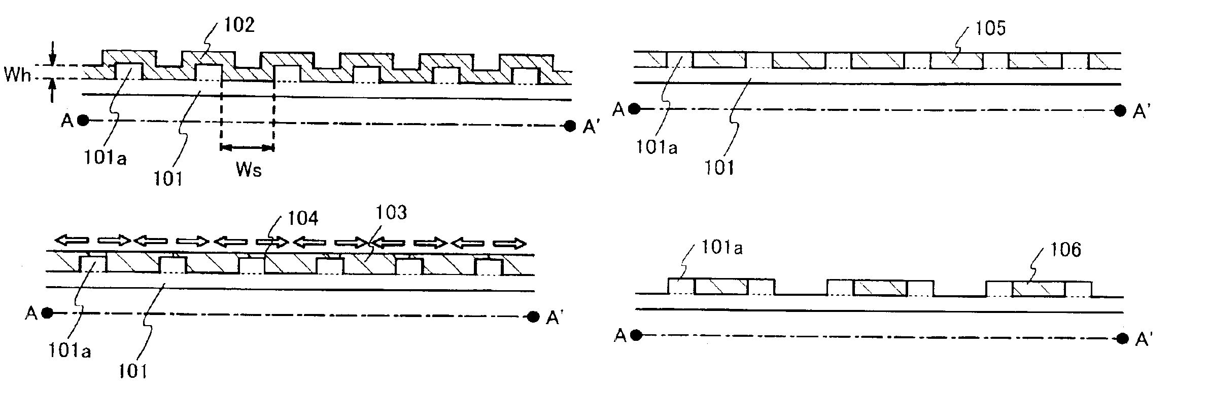
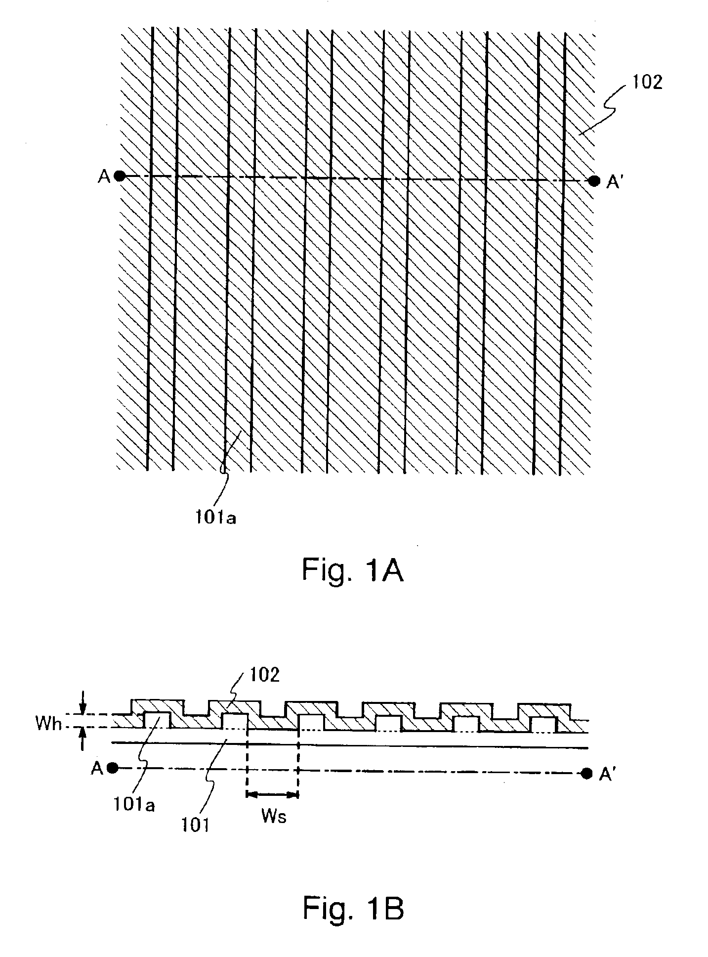
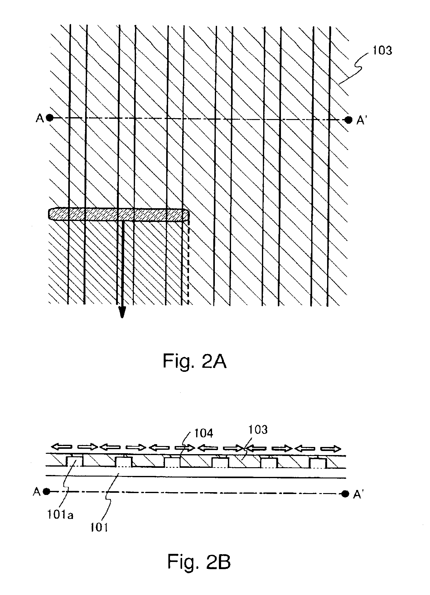
[0130]First, the film is formed following the steps in the embodiment mode up to the state of FIGS. 2A and 2B. Then, as shown in FIG. 6A, a mask 170 is used to cover all the film other than the portion serving as the channel formation region of the TFT in the subsequent steps. In this state, the surface of the semiconductor film 103 is being etched to expose the upper surface of the projective portion 101a of the base film 101. Note that FIG. 6B is a sectional view taken along the dashed line B-B′ of FIG. 6A and FIG. 6C is a sectional view taken along the dashed line C-C′ of FIG. 6A. Through the above steps, a semiconductor film 171 exiting in the depressive portion of the base film 101 is formed. The removal of the semiconductor film 103 from the upper surface may be formed by any method and in this embodiment, etching is us...
embodiment 2
(Embodiment 2)
[0135]In this embodiment, a description will be made of a case in which in the embodiment mode, after the island-like semiconductor film is formed, the projective portion is removed.
[0136]First, the film is formed following the steps in the embodiment mode up to the state of FIGS. 35A and 35B. In this embodiment, however, it is important to form the base film having such a structure as to remove only the projective portion by etching or the like. The base film to be used in this embodiment consists of a first base film made of silicon nitride, a rectangular second base film made of silicon oxide, and a third base film made of silicon oxide. The second base film is formed on the first base film and the third base film is formed so as to cover the first and second base films. Note that the structure of the base film is not limited to this and any structure can be adopted provided that it enables the removal of the projective portions alone by etching or the like.
[0137]Al...
embodiment 3
(Embodiment 3)
[0142]On the base film in which the plural projective portions of a rectangular or stripe shape are arranged at substantially the same interval, the semiconductor film is formed and is irradiated with the laser light in the longitudinal direction of the projective portions. Then, the grain boundary may develop obliquely between the projective portion formed at the outermost position and the adjacent projective portion in some cases.
[0143]FIG. 8 or FIG. 38 is a top view of the semiconductor film when on the base film in which the plural projective portions of a rectangular or stripe shape are arranged in parallel at substantially the same interval, the semiconductor film is formed and is irradiated with the laser light in the longitudinal direction of the projective portions. In this embodiment, a case of using a base film in which five rectangular projective portions 130a to 130e are arranged in parallel is shown. The projective portions 130a to 130e are arranged in pa...
PUM
 Abstract
Description
Claims
Application Information