Method of separating thin film device, method of transferring thin film device, thin film device, active matrix substrate and liquid crystal display device

a technology of thin film and liquid crystal display, which is applied in the direction of optics, transistors, instruments, etc., can solve the problems of insufficient separation phenomenon of separation layer and laminate relation of layer to be transferred, so as to prevent deterioration in characteristics, accelerate separation phenomenon, and reduce the quantity of light inciden

Inactive Publication Date: 2005-04-26
SAMSUNG ELECTRONICS CO LTD
View PDF26 Cites 146 Cited by
  • Summary
  • Abstract
  • Description
  • Claims
  • Application Information

AI Technical Summary

Benefits of technology

[0025](3) The third step described above in (2) preferably includes the step of irradiating the separation layer with light. This can gasify the separation ion by the light. At this time, irradiation of the substrate from the rear side thereof can decrease the quantity of light incident on the thin film device layer and prevent deterioration in characteristics thereof.
[0026](4) In the ion implantation step, bonds of atoms or molecules which constitute the separation layer are preferably cut by the ions to previously damage the separation layer. This accelerates the separation phenomenon in the separation layer, which is caused in the subsequent separation step.
[0027](5) In the ion implantation step, the characteristics of the separation layer are preferably changed to previously weaken adhesion between the separation layer and the substrate. This facilitates the separation phenomenon in the separation layer, which is caused in the subsequent separation step.

Problems solved by technology

As a result of experiments, it was found that in some cases of separating the thin film device from the first substrate, a separation phenomenon does not sufficiently occur in the separation layer only by irradiating the separation layer with light, for example.
There was also a problem in which the laminate relation of the layer to be transferred to the first substrate used in production of the layer to be transferred differs from the laminate relation of the layer to be transferred to the second substrate to which the layer to be transferred is transferred.

Method used


Image

  • Method of separating thin film device, method of transferring thin film device, thin film device, active matrix substrate and liquid crystal display device
  • Method of separating thin film device, method of transferring thin film device, thin film device, active matrix substrate and liquid crystal display device
  • Method of separating thin film device, method of transferring thin film device, thin film device, active matrix substrate and liquid crystal display device

Examples


example 1

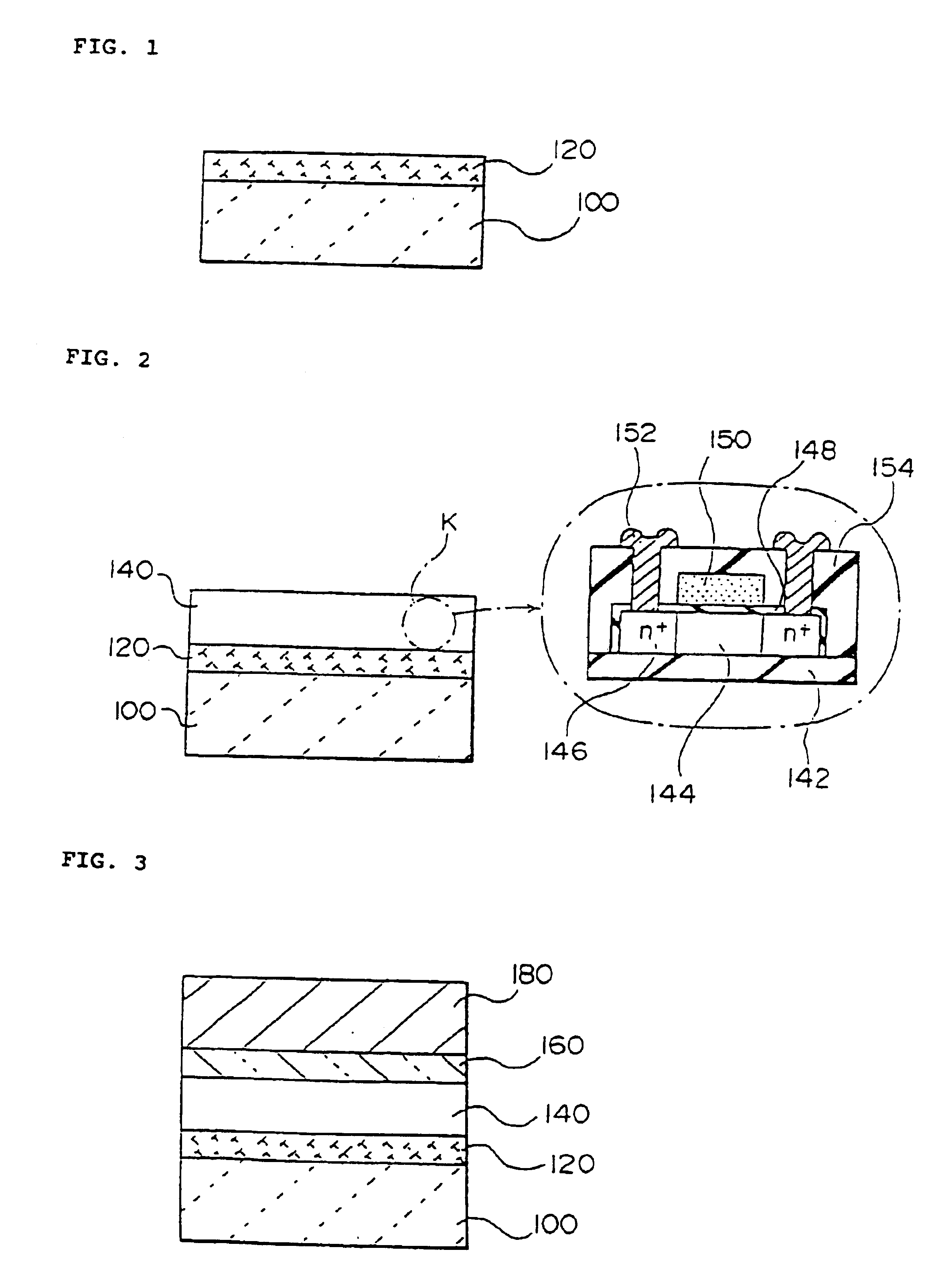
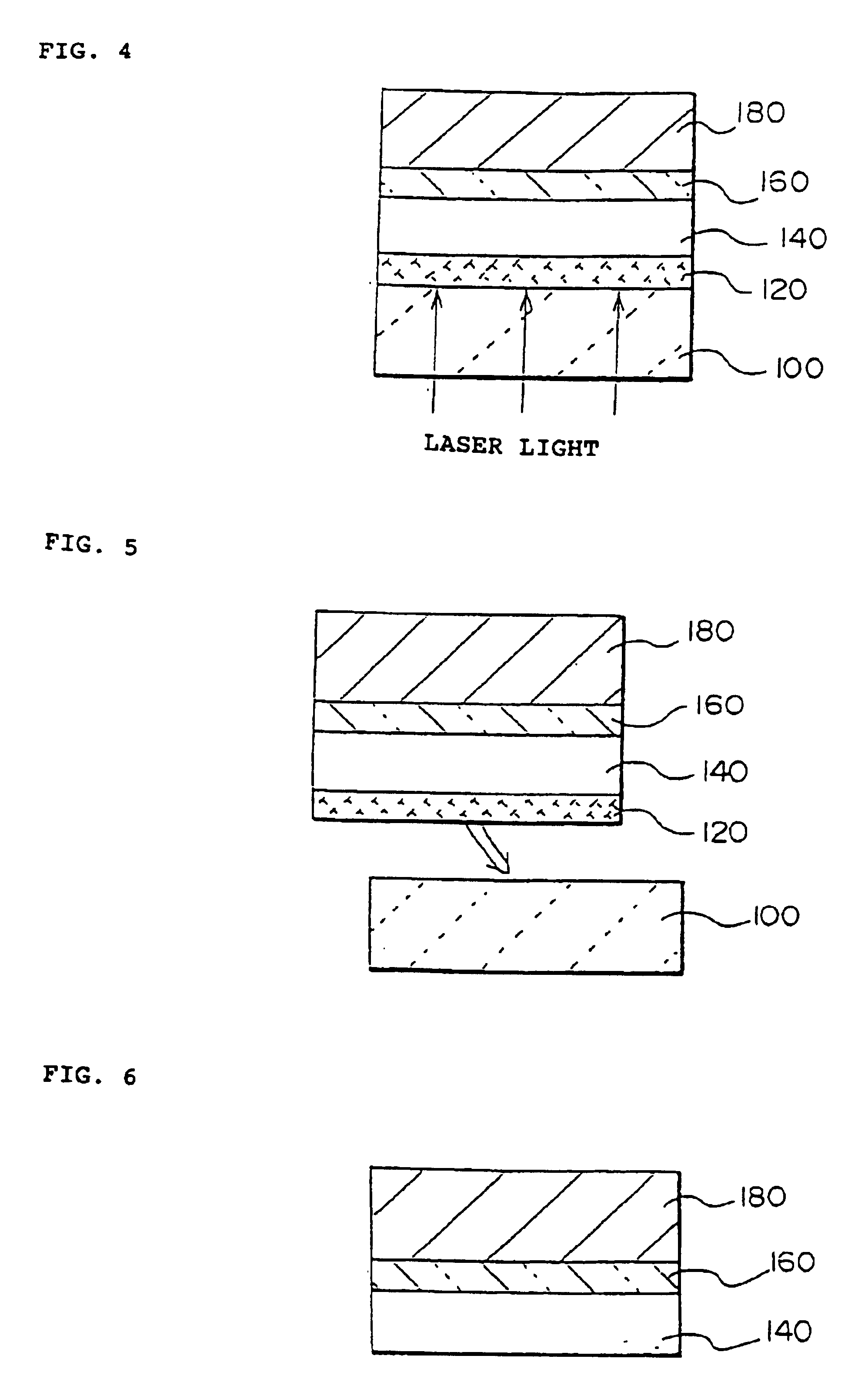
[0277]A quartz substrate (softening point: 1630° C., strain point: 1070° C., transmittance for excimer laser: about 100%) of 50 mm long×50 mm wide×1.1 mm thick was prepared, and an amorphous silicon (a-Si) film was formed as a separation layer (laser absorbing layer) on one side of the quartz substrate by the low-pressure CVD method (Si2H6 gas, 425° C.). The thickness of the separation layer was 100 nm.

[0278]Next, a SiO2 film was formed as an intermediate layer by the ECR-CVD method (SiH4+O2 gas, 425° C.) on the separation layer. The thickness of the intermediate layer was 200 nm.

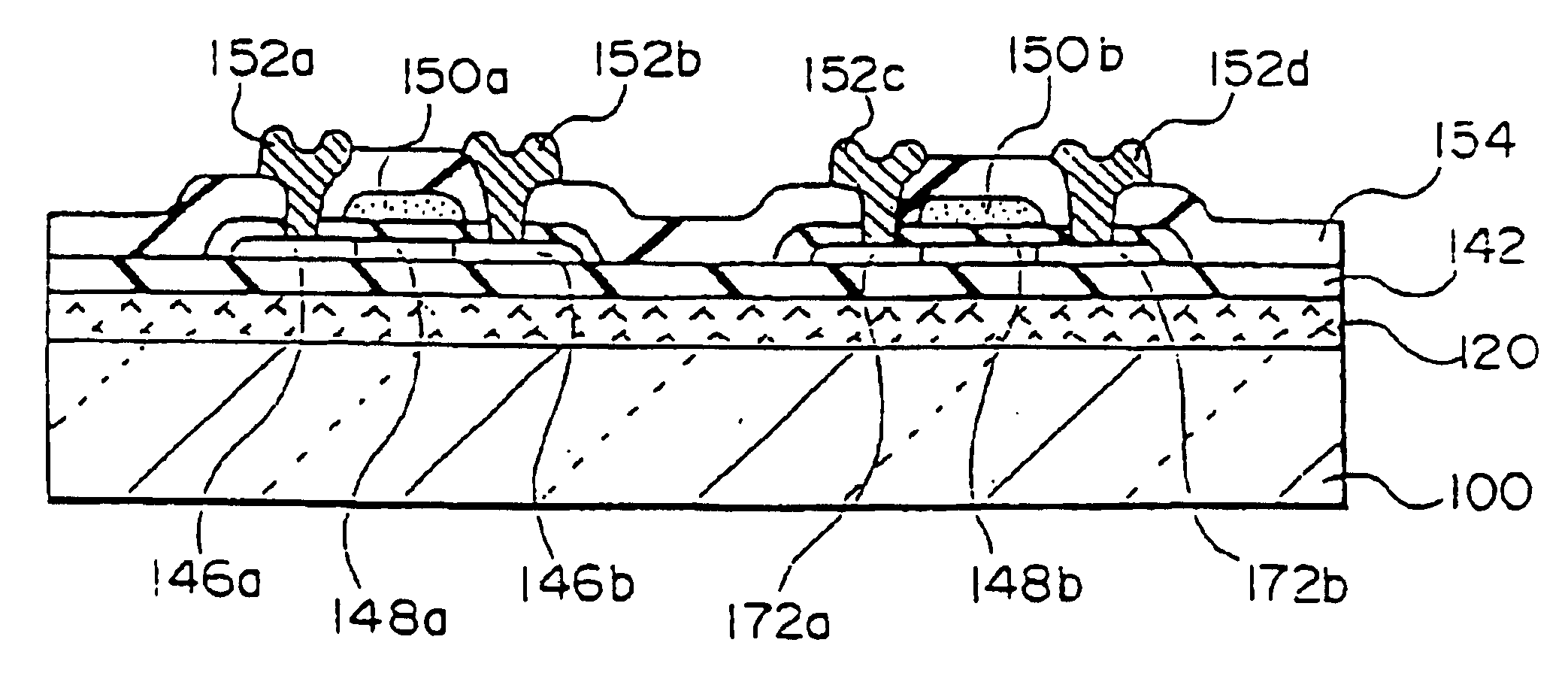
[0279]Next, an amorphous silicon film having a thickness of 50 nm was formed as a layer to be transferred on the intermediate layer by the low-pressure CVD method (Si2H6 gas, 425° C.), and then crystallized by irradiation of laser light (wavelength 308 nm) to form a polysilicon film. Then, the polysilicon film was subjected to predetermined patterning to form regions serving as source, drain and channel of ...

example 2

[0285]The same transfer of a thin film transistor as Example 1 was repeated except that the separation layer comprised an amorphous silicon film containing 20 at % of H (hydrogen) and formed by the separation layer forming process.

[0286]The H content of the amorphous silicon film was adjusted by appropriately setting deposition conditions of the low-pressure CVD method.

example 3

[0287]The same transfer of a thin film transistor as Example 1 was repeated except on layer comprised a ceramic thin film (composition: PbTiO3, thickness: 200 nm) formed by the sol-gel method using spin coating.


PUM

PropertyMeasurementUnit
temperatureaaaaaaaaaa

Abstract

A separation layer is provided on a substrate, and a thin film device, such as TFT, is formed thereon. Separation accelerating ions such as hydrogen ions are implanted into the separation layer in the course of the process for forming the thin film device. After the formation of the thin device, the thin film device is preferably joined to a transfer material through an adhesive layer, and irradiated with laser light from the substrate side. This causes separation in the separation layer by also using the action of the separation acceleration ions. The thin film device is separated from the substrate. This permits transfer of a desire thin film device to any substrate.

Description

BACKGROUND OF THE INVENTION[0001]1. Field of Invention[0002]The present invention relates to a method of separating a thin film device, a method of transferring a thin film device, a thin film device, an active matrix substrate and a liquid crystal display device.[0003]2. Description of Related Art[0004]For example, the production of a liquid crystal display using a thin film transistor (TFT) is carried out through the step of forming the thin film transistor on a substrate by CVD or the like. The step of forming the thin film transistor on the substrate is accompanied by high-temperature treatment, and it is thus necessary to use a substrate made of a material having excellent heat resistance, i.e., high softening point and melting point. Therefore, at present, quartz glass is used as a substrate which can resist a temperature of about 1000° C., and heat-resistant glass is used as a substrate which can resist a temperature of about 500° C.[0005]As described above, the substrate on ...

Claims


Application Information

Patent Timeline
Patent Type & Authority Patents(United States)
IPC IPC(8): H01L21/762H01L21/70H01L27/12H01L21/84H01L29/786G02F1/136G02F1/1368H01L21/336H01L21/68H01L21/77
CPCH01L21/6835H01L21/76254H01L27/1214H01L27/1266H01L29/66757G02F2001/13613H01L2924/3511H01L2221/6835H01L2221/68359H01L2221/68363H01L2221/68368H01L2924/3025H01L2221/68318G02F1/13613H01L29/786
Inventor INOUE, SATOSHISHIMODA, TATSUYA
Owner SAMSUNG ELECTRONICS CO LTD
Why Eureka
Try Eureka