Tuneable ferroelectric decoupling capacitor

a ferroelectric decoupling capacitor and ferroelectric technology, applied in the direction of capacitors, semiconductor devices, electrical equipment, etc., can solve the problems of destroying the efficacy of bypass capacitors, becoming nearly impossible to escape harmonics or subharmonics, etc., to achieve maximum damping and maximum losses

Inactive Publication Date: 2005-05-03
GLOBALFOUNDRIES INC
View PDF15 Cites 105 Cited by
  • Summary
  • Abstract
  • Description
  • Claims
  • Application Information

AI Technical Summary

Benefits of technology

[0004]Now, an improved bypass capacitor has been developed for attachment to a semiconductor integrated circuit chip or module, which can be designed with mechanical dimensions or by electrical bias to provide maximum losses at selected frequencies. The capacitor can be engineered to provide maximum damping at the resonant frequency of the bypass network, the clock frequency of the semiconductor integrated circuit (IC) chip, or some multiple or submultiple of the clock frequency of the IC chip.

Problems solved by technology

Thus, it becomes nearly impossible to escape harmonics or subharmonics that can excite the resonant frequency of the bypass capacitor and its ancillary inductance.
Adding resistance to the inductance to provide critical damping, destroys the efficacy of the bypass capacitor.

Method used


Image

  • Tuneable ferroelectric decoupling capacitor
  • Tuneable ferroelectric decoupling capacitor
  • Tuneable ferroelectric decoupling capacitor

Examples


example 1

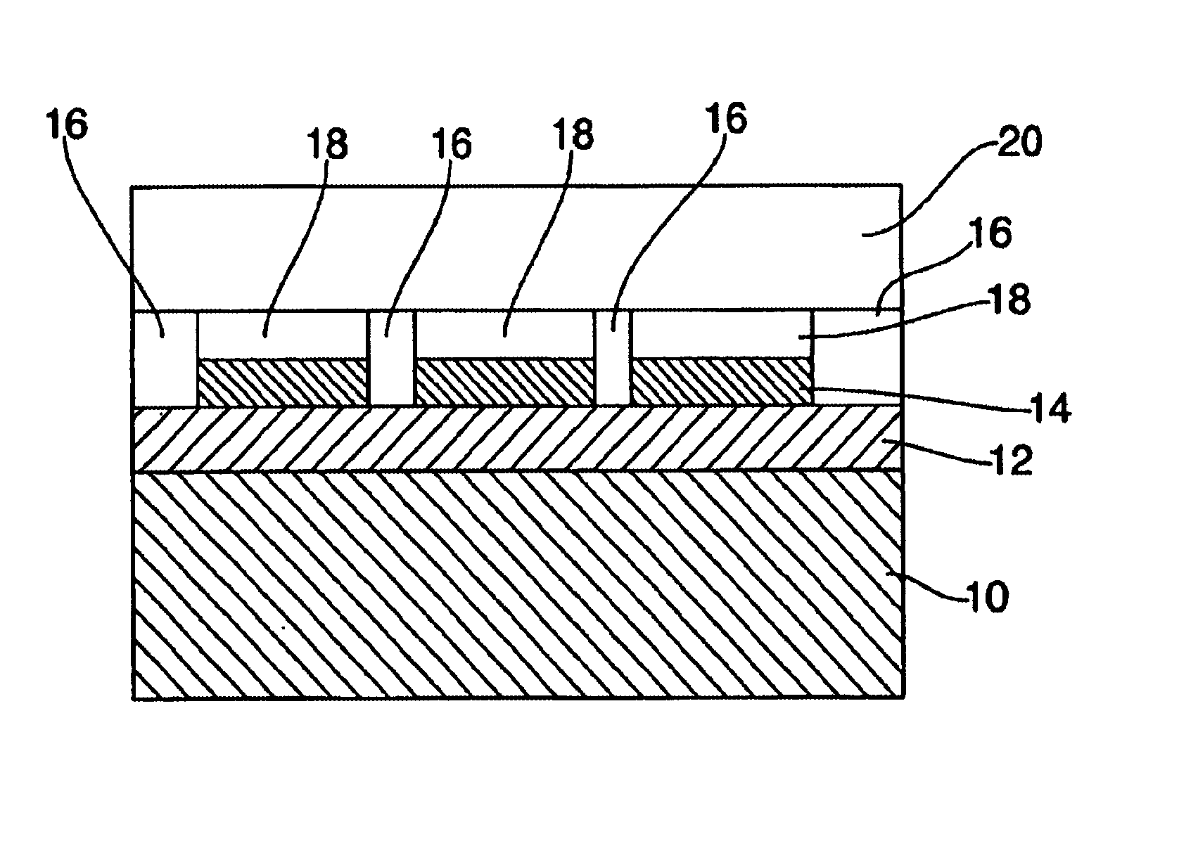
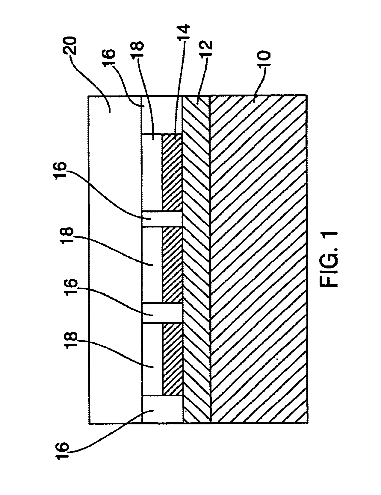
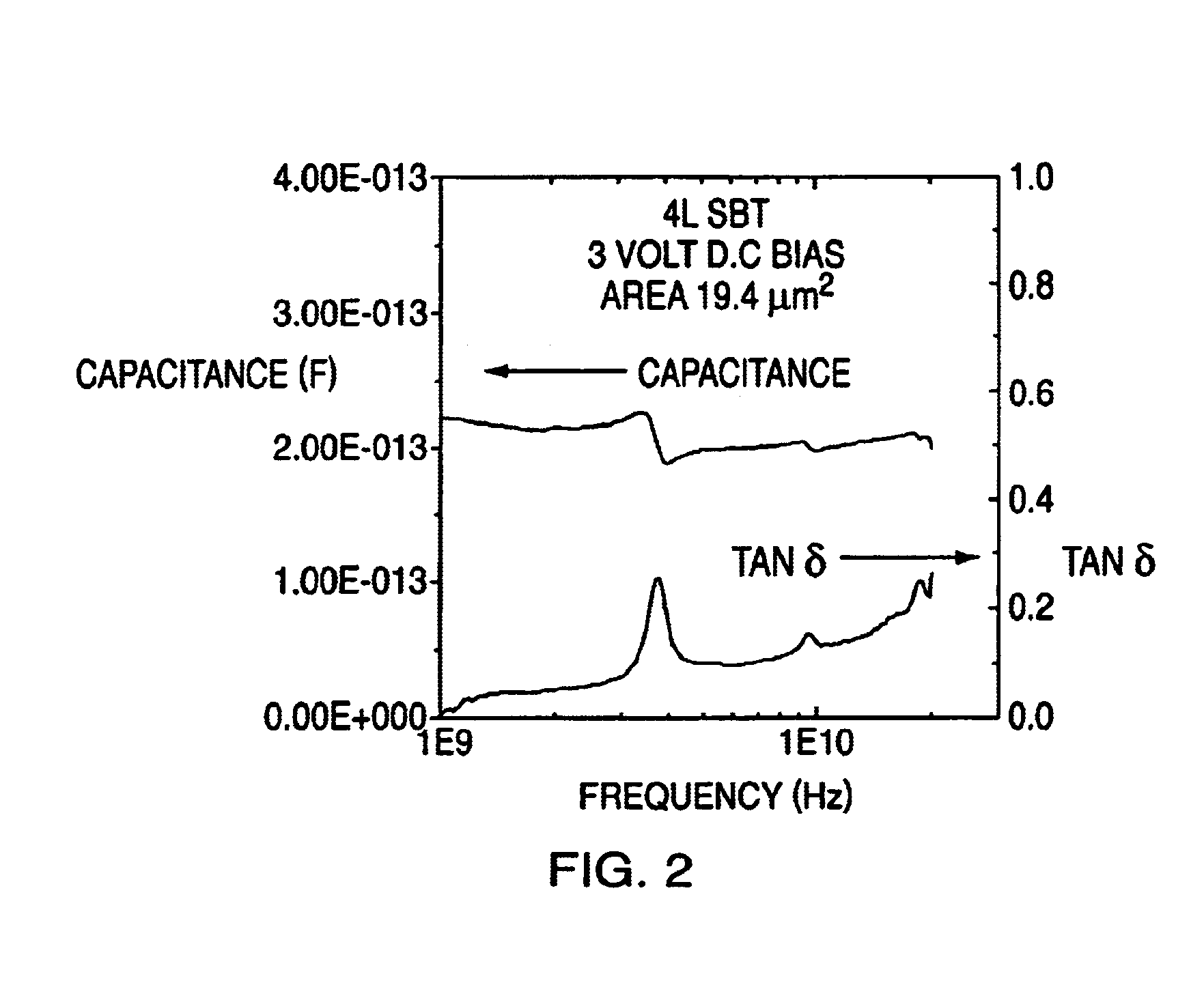
[0017]This example illustrates a 4 micrometer by 4 micrometer ferroelectric capacitor prepared on an oxidized silicon wafer. An oxide layer 400 nm thick was deposited on a silicon wafer. A blanket layer 250 nm thick of platinum was sputtered on the wafer and patterned by standard photolithiographic techniques to form a bottom electrode for the capacitor and a contact pad for electrical testing. A thin film consisting of Strontium Bismuth Tantalate (SBT) / Bismuth Titanate (BT) ferroelectric layers was spun onto the wafer by chemical solution deposition technique. The film consisted of three layers SBT and one layer of BT and has a total thickness of 120 nm. A blanket film 100 nm thick of Pt was deposited on top of the film and patterned to form the top capacitor electrode and electrical contact.

[0018]Measurements made using a Radiant Technologies ferroelectric test system confirmed that the film was ferroelectric. High frequency electrical testing was conducted using a Hewlett Packard...

example 2

[0022]This example illustrates a capacitor prepared from a substrate on which a blanket conducting electrode is deposited made of a noble metal such as platinum, a ferroelectric layer is deposited on the electrode by a process such as chemical vapor deposition (CVD), physical vapor deposition (PVD), or chemical solution deposition (CSD). Ferroelectric materials with large piezoelectric coefficients such as lead zirconium titanate (PZT) are preferred. A second conducting electrode is deposited on the ferroelectric to form a capacitor stack. The stack is patterned into an array of capacitors by standard lithographic techniques. The lateral dimensions of the capacitors are chosen so that individual capacitors have resonances at the desired frequency / frequencies. The thickness of the ferroelectric and the number of the capacitors are chosen so as to provide the required capacitance per chip (1 nF typical). For PZT, which has a dielectric constant of about 1000 at a film thickness of 200...


PUM


Abstract

A voltage supply bypass capacitor for use with a semiconductor integrated circuit chip or module comprising a ferroelectric dielectric having electromechanical properties designed to provide maximum losses at selected frequencies.

Description

[0001]This application is a division of application Ser. No. 09 / 430,901, filed Nov. 1, 1999, which is now U.S. Pat. No. 6,507,476BACKGROUND[0002]High performance integrated circuit chips such as microprocessors require large values of bypass capacitance located closely adjacent to the chip. In some recent designs, such as the Digital Equipment Corporation Alpha 600 MHz microprocessor, it has been necessary to wirebond the bypass capacitor directly to the chip. In this particular example, the “bypass capacitor” is itself a specialized P channel FET chip with a large thin oxide region. Capacitor values are typically 10 nanofarads or more. Practical values of inductance range from a fraction of a nanohenry to a few nanohenrys. A simple calculation shows that such circuit combinations lead to resonant frequencies very close to the clock frequency of the microprocessor. The microprocessor clock itself contains many harmonics of the basic clock frequency. Specific repetitive operations of...

Claims


Application Information

Patent Timeline
Patent Type & Authority Patents(United States)
IPC IPC(8): H01L27/08H01L21/02
CPCH01L27/0805H01L28/55
Inventor SHAW, THOMAS M.PRICER, W. DAVIDNEUMAYER, DEBORAH A.BANIECKI, JOHN D.LAIBOWITZ, ROBERT B.
Owner GLOBALFOUNDRIES INC
Why Eureka
Try Eureka