Metal-oxide-semiconductor device formed in silicon-on-insulator

US6890804B1Active Publication Date: 2005-05-10BELL SEMICON LLC

Image

  • Metal-oxide-semiconductor device formed in silicon-on-insulator
  • Metal-oxide-semiconductor device formed in silicon-on-insulator
  • Metal-oxide-semiconductor device formed in silicon-on-insulator

Examples


Embodiment Construction

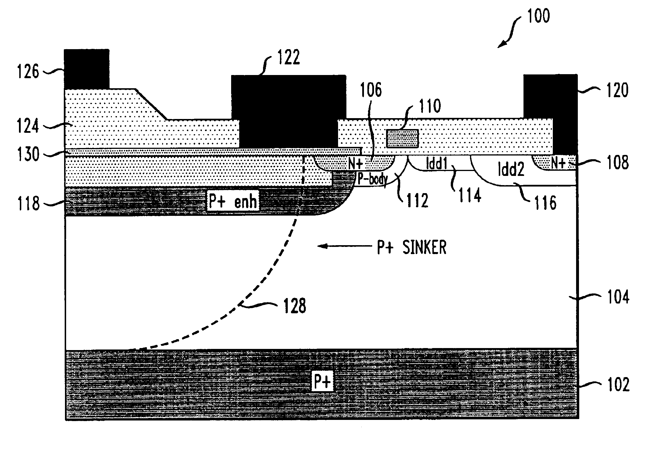
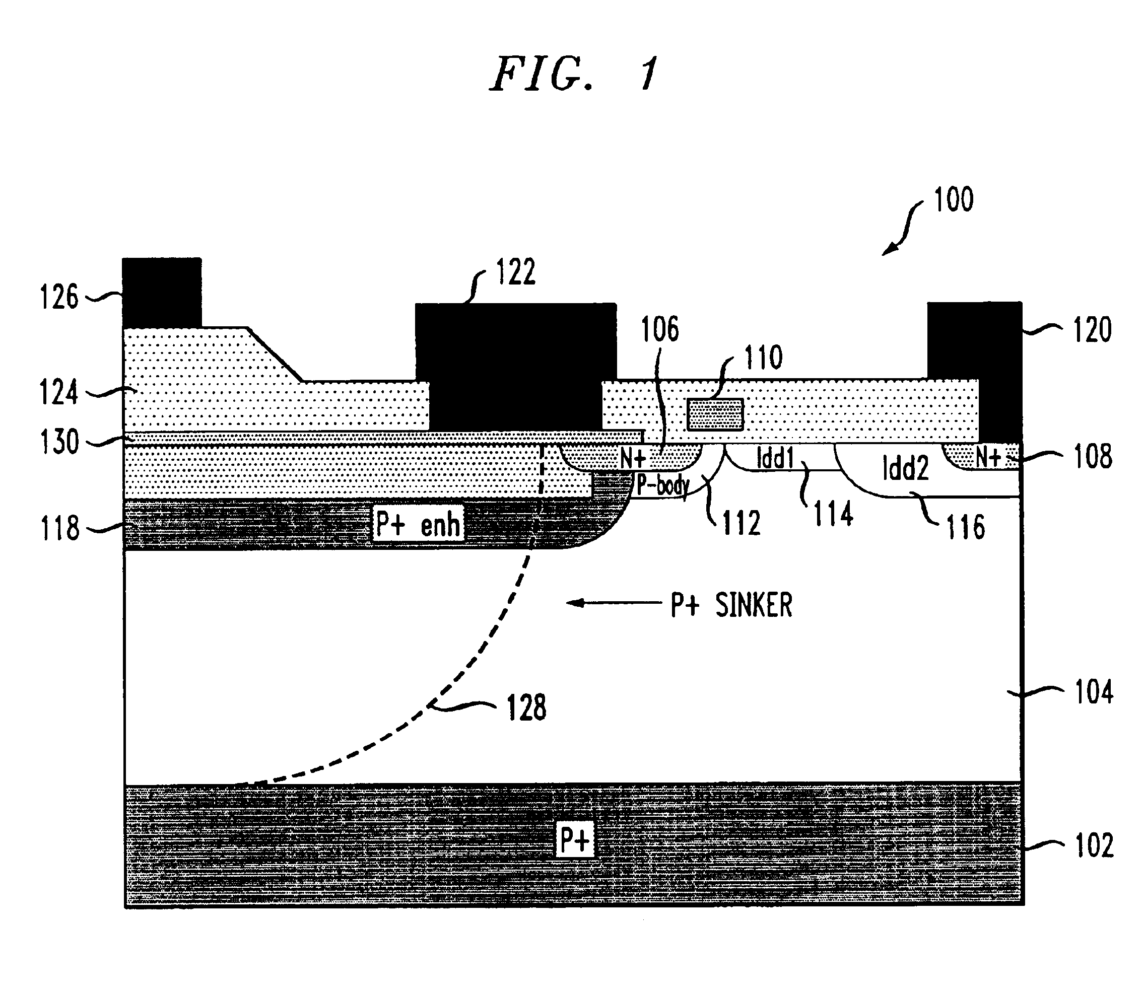
[0013]The present invention will be described herein in the context of an illustrative MOS integrated circuit fabrication technology suitable for forming discrete RF LDMOS transistors, as well as other devices and / or circuits. It should be appreciated, however, that the present invention is not limited to the fabrication of this or any particular device or circuit. Rather, the invention is more generally applicable to techniques for forming a semiconductor device in partial SOI having improved performance and reliability.

[0014]Although implementations of the present invention are described herein with specific reference to an LDMOS device and a complementary metal-oxide-semiconductor (CMOS) fabrication process, it is to be appreciated that the techniques of the present invention are similarly applicable to other fabrication processes (e.g., bipolar) and / or the formation of other devices, such as, but not limited to, an MOS field-effect transistor (MOSFET), a bipolar junction transis...


PUM


Abstract

A semiconductor device includes a substrate of a first conductivity type, an insulating layer formed on at least a portion of the substrate, and an epitaxial layer of a second conductivity type formed on at least a portion of the insulating layer. First and second source / drain regions of the second conductivity type are formed in the epitaxial layer proximate an upper surface of the epitaxial layer, the first and second source / drain regions being spaced laterally from one another. A gate is formed above the epitaxial layer proximate the upper surface of the epitaxial layer and at least partially between the first and second source / drain regions. The device further includes a first source / drain contact formed through the epitaxial layer and insulating layer, the first source / drain contact configured so as to be in direct electrical connection with the substrate, the first source / drain region and the epitaxial layer, and a second source / drain contact formed through the epitaxial layer, the second source / drain contact configured so as to be in direct electrical connection with the second source / drain region.

Description

FIELD OF THE INVENTION[0001]The present invention relates generally to metal-oxide-semiconductor (MOS) devices, and more particularly relates to techniques for fabricating an improved MOS device in silicon-on-insulator (SOI).BACKGROUND OF THE INVENTION[0002]Power MOS devices, including lateral diffused MOS (LDMOS) devices, are generally difficult to manufacture in SOI, although the benefits of using an SOI process to enhance the high-frequency performance of discrete or integrated LDMOS devices, particularly in a radio frequency (RF) range of operation (e.g., above one gigahertz), are known.[0003]In an article by J. Cai et al., “A Partial SOI Technology for Single-Chip RF Power Amplifiers,” IEEE IEDM, pp. 40.3.1-40.3.4, 2001, a process is described for building an RF LDMOS device in partial SOI by employing multiple trench and dielectric etching to form thin “walls” of silicon, and then oxidizing these walls to form one layer of SOI under the drain region of the RF LDMOS device and ...

Claims


Application Information

Patent Timeline
10 May 2005
Publication
US6890804B1
IPC
H01L29/76; H01L21/70; H01L29/66; H01L29/786; H01L21/84; H01L21/336; H01L29/417; H01L29/78
CPC
H01L29/41741; H01L29/66772; H01L29/78645; H01L29/78609; H01L29/78624; H01L29/7835; H01L29/402; A61P31/04
Inventors
SHIBIB, MUHAMMED AYMAN; XU, SHUMING