
EL device

a technology of a device and a discharge tube, applied in the field of el devices, can solve the problems of low yield, low yield, and high applied driving voltage needed for the device to emit light, and achieve the effect of stable light emission performan

Inactive Publication Date: 2005-05-10
IFIRE IP CORP
View PDF28 Cites 23 Cited by
  • Summary
  • Abstract
  • Description
  • Claims
  • Application Information

AI Technical Summary

Benefits of technology

"The present invention provides an EL device that has a low emission start voltage and driving voltage, and stable light emission performance. This is achieved by using an insulator layer with high dielectric strength and low susceptibility to change with time, and a high relative permittivity. The insulator layer contains barium titanate and magnesium oxide, manganese oxide, yttrium oxide, barium oxide, calcium oxide, and silicon oxide in a specific ratio. The electrical insulating substrate and the first insulator layer are each formed of a ceramic material. The invention also includes the use of BaO, CaO, and SiO2 in a specific form. The first electrode is formed of at least one metal selected from Ni, Cu, W, and Mo or an alloy composed mainly of at least one metal selected from these metals."

Problems solved by technology

However, such a device has some practical problems.
One problem is that it is difficult to reduce the dielectric breakdown of the device to nil over a wide area, resulting in low yields, and another is that the applied driving voltage necessary for the device to emit light becomes high because voltage is dividedly applied to the insulator layers.
However, the temperature of the substrate must be elevated to about 600° C. for PbTiO3 film formation, and so it is difficult to apply the PbTiO3 film to the fabrication of hitherto thin-film EL devices using a glass substrate.
This film is formed at 400° C. However, the practical use of the film for a thin-film EL device using a glass substrate offers a problem because an ITO transparent electrode is reduced and blackened during film formation by sputtering.
In this case, however, the substrate costs much, and the upper limit to the treatment temperature is again 600° C. as well.
However, the ITO film is susceptible to dielectric breakdown at its edge because of the insufficient dielectric strength of such thinner insulator layers.
This is an obstacle to development of large-area and large-capacity displays.
Thus, a conventional thin-film EL device must be driven at high voltage, resulting in the need of using a costly driving circuit of high dielectric strength.
This unavoidably makes displays costly and large-area displays hardly achievable.
However, this material must be used with an increased thickness because of its insufficient dielectric strength.

Method used


Image

  • EL device
  • EL device

Examples


example

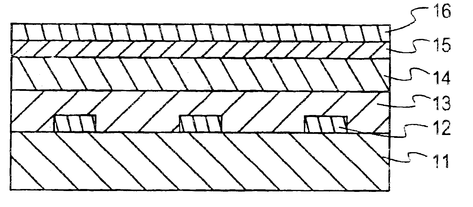
[0074]A binder was mixed with a mixture of Al2O3 powders with SiO2, MgO and CaO powdery additives to prepare a paste, which was then cast into a green sheet forming a ceramic substrate of 1 mm in thickness. Using a screen printing process, a Ni paste was formed on this ceramic precursor according to a striped pattern of 0.3 mm in width, 0.5 mm in pitch and 1 μm in thickness. For the material for the first insulator layer, a paste containing pre-fired powders having the composition shown in Table 1 was prepared, This paste was then printed all over the surface of the green sheet with the electrode pattern formed thereon. The post-firing thickness of the printed paste was 4 μm.

[0075]

TABLE 1Composition of Dielectric MaterialBreakdownFilmEmissionSampleMgOMnO(Ba, Ca)SiO2Y2O3FieldThicknessStart VoltageNo.(mole)(mole)(wt %)(Mole)ε s(MV / m)(μm)(V)110.1950.042850150452.8210.37550.272530150453.0310.1950.182920150452.7410.37550.272690150452.9510.37550.093040150452.7610.375503070150452.77 (compa...


PUM

PropertyMeasurementUnit
thicknessaaaaaaaaaa
average crystal grain diameteraaaaaaaaaa
dielectric strengthaaaaaaaaaa

Abstract

The EL device of the present invention has a structure in which a first electrode, a first insulator layer, an electroluminescence-producing light emitting layer, a second insulator layer, and a second electrode layer are successively stacked on an electrical insulating substrate. At least one of the first insulator layer and the second insulator layer has as a main component barium titanate and in addition 0.1 to 3 mole % magnesium oxide, 0.05 to 1.0 mole % manganese oxide, no more than 1 mole % yttrium oxide, 2 to 12 mole % of barium oxide and calcium oxide, and 2-12 mole % silicon oxide.

Description

CROSS-REFERENCE TO RELATED APPLICATIONS[0001]This application is a continuation and claims priority to International Application No. PCT / JP00 / 02231 filed Apr. 6, 2000 and Japanese Application No. 11-101195, filed Apr. 8, 1999, and the entire content of both applications is hereby incorporated by reference.TECHNICAL FIELD[0002]The present invention relates to an EL device preferably used as a thin yet flat form of display means.BACKGROUND OF ART[0003]An EL device comprising a light emitting layer formed of an inorganic compound and interleaved between upper and lower insulator thin films is excellent in luminance characteristics and stability upon driven on AC current. EL devices fabricated through a fabrication process where all process steps are carried out with thin-film technologies are now used for a variety of displays. One basic arrangement of such a light emitting device is shown in FIG. 2.[0004]This light emitting device has on a glass substrate 21 a multilayered film struct...

Claims


Application Information

Patent Timeline
Patent Type & Authority Patents(United States)
IPC IPC(8): H05B33/26H05B33/02H05B33/22H05B33/12C04B35/46
CPCH05B33/02H05B33/12H05B33/26H05B33/22Y10S428/917
Inventor NAGANO, KATSUTONOMURA, TAKESHITAKEISHI, TAKUTAKAYAMA, SUGURU
Owner IFIRE IP CORP
Learn More