Analog demultiplexer

a multi-channel, analog technology, applied in the direction of pulse technique, instrument, color signal processing circuit, etc., can solve problems such as unsatisfactory effects, and achieve the effect of improving switching speed

Active Publication Date: 2005-05-24
INTERSIL INC
View PDF7 Cites 16 Cited by
  • Summary
  • Abstract
  • Description
  • Claims
  • Application Information

AI Technical Summary

Benefits of technology

[0042]To improve switching speed in one embodiment, the switches S1a, S1b, etc. are formed from as a CMOS switch made from a combined PMOS and NMOS transmission gate. The NMOS transistor enables the circuit to switch fast, while the PMOS transistor being on after the circuit settles removes voltage offset typically existing with onl

Problems solved by technology

When the output of amplifier A1 rings,

Method used


Image

  • Analog demultiplexer
  • Analog demultiplexer
  • Analog demultiplexer

Examples


Embodiment Construction

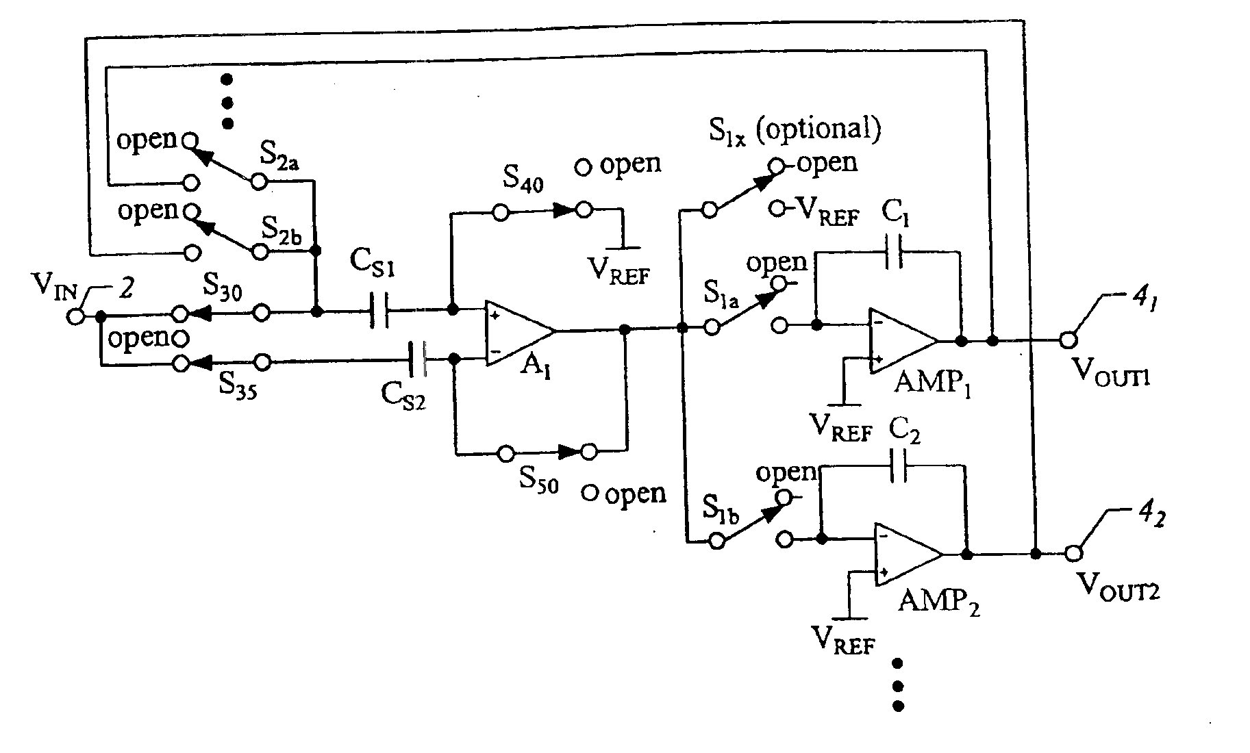
[0058]An approach for an analog demultiplexer in accordance with the present invention is shown in FIG. 6. Using this circuit and switching S1a, S1b . . . etc. and S2a, S2b . . . etc., control logic can guide VIN to be sampled and held on a specific one of the output buffers AMP1-AMPN. Note that FIG. 6 shows use of multiple switches S1a, S1b . . . etc. and S2a, S2b . . . etc., as an alternative, a single switch could be used for all of switches S1a, S1b . . . etc. or S2a, S2b . . . etc. However, use of multiple switches permits the input amplifier A1 to be connected to more than one of the output amplifiers AMP1-AMPN at one time. Further note that although switches such as S1a and S2a typically open and close together simultaneously in prior art designs, in the present invention the switches may or may not close simultaneously.

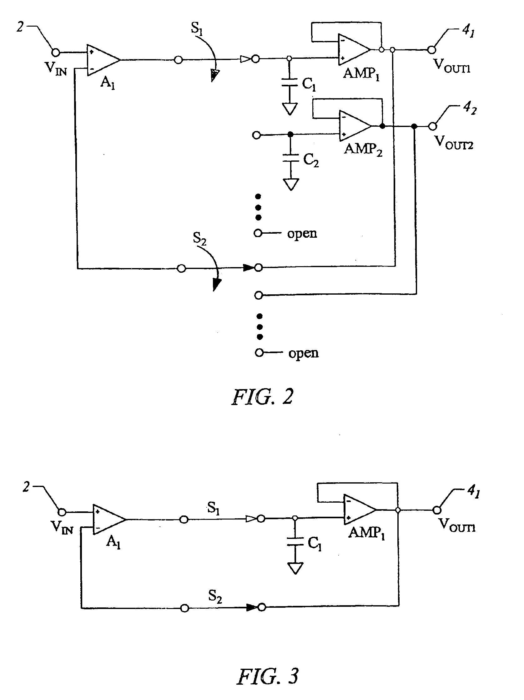
[0059]For a description of operation, to simplify the system of FIG. 6, FIG. 7 is included showing only two amplifiers, assuming VIN is to be sampled to an ou...


PUM


Abstract

The analog demultiplexer (FIG. 6) includes an input amplifier (A1), and output amplifiers (AMP1-AMPN). The output and inverting (−) input of amplifiers (AMP1-AMPN) are connected by a respective capacitor (C1-CN). Switches (S1a, S1b, etc.) connect the output of amplifier (A1) to the inverting input of one of (AMP1-AMPN). Switches (S2a, S2b, etc.) connect the output of one of (AMP1-AMPN) to the non-inverting input of the amplifier A1. Switches (S2a, S2b, etc.) and (S1a, S1b, etc.) open and close together in pairs. With feedback from the output of (AMP1-AMPN) through (A1), the gain and any offset of (AMP1-AMPN) is divided down by the gain of (A1). Amplifier (A1) has capacitors (CS1 and CS2) connected to its inputs. Switch (S50) connects the inverting input of amplifier (A1) to its output, and switch (S40) connects the non-inverting input of (A1) to a voltage reference (VREF) matching (VREF) applied to (AMP2). Switches (S30) and (S35) connect (CS1) and (CS2) to the demultiplexer input (2). In operation, switches (S40, S50, S30 and S35) are initially closed, while switches (S2a, S2b, etc.) are open to charge both capacitors (CS1) and (CS2) and the inputs and output of (A1) to (VREF). Switch (S50) provides feedback to divide down gain errors and offset of (A1). Switches (S30, S35, S40 and S50) are then open, while one of switches (S2a, S2b, etc.) is closed with one switch (S1a, S1b, etc) to drive one of the output voltages (VOUT1-VOUTN). With inputs and outputs of (A1) and the connected (AMP1-AMPN) initially be at (VREF), very little settling time is needed.

Description

CLAIM OF PRIORITY TO PROVISIONAL APPLICATION[0001]This application claims priority to provisional application SC / Ser. No. 60 / 317,482, entitled “Analog Demultiplexer” filed Sep. 5, 2001.CROSS REFERENCE TO RELATED APPLICATION[0002]U.S. patent application Ser. No. 10 / 236,211 (now U.S. Pat. No. 6,781,532) entitled “Simplified Multi-Output Digital to Analog Converter (DAC) for a Flat Panel Display” filed simultaneously with this application on Sep. 5, 2002 is incorporated herein by reference.[0003]U.S. patent application Ser. No. 10 / 896,275 entitled “Simplified Multi-Output Digital to Analog Converter (DAC) for a Flat Panel Display” filed on Jul. 21, 2004.BACKGROUND[0004]1. Technical Field[0005]The present invention relates to analog demultiplexer for distributing signals from a single input line to one of multiple output lines. In particular, the present invention relates to an analog demultiplexer for distributing a video input signal to one of several video display column drivers, wit...

Claims


Application Information

Patent Timeline
IPC IPC(8): H03K17/693H03K17/16H03K17/00H03F3/72
CPCH03K17/007H03K17/693H03K17/162H03K17/62
Inventor CHIA, CHOR-YIN
Owner INTERSIL INC
Why Eureka
Try Eureka