Trench semiconductor device having gate oxide layer with multiple thicknesses and processes of fabricating the same

a technology of gate oxide layer and mosfet, which is applied in the direction of semiconductor devices, diodes, electrical devices, etc., can solve the problems of affecting the operation of the device, affecting the reliability of the device, and unable to guarantee the net overlap of the polysilicon gate into the drain region, so as to reduce the strength of the electric field and reduce the capacitance

Inactive Publication Date: 2005-05-31
ADVANCED ANALOGIC TECHNOLOGIES INCORPORATED
View PDF8 Cites 30 Cited by
  • Summary
  • Abstract
  • Description
  • Claims
  • Application Information

AI Technical Summary

Benefits of technology

[0029]In accordance with this invention, a trench-gated semiconductor device is formed, having a dielectric layer separating the gate electrode from the semiconductor material surrounding the trench wherein the thickness of the dielectric layer is greater in a region at the bottom of the trench. This structure helps to reduce the strength of the electric field near the bottom of the trench, particularly at the corner or rounded portion where the bottom of the trench makes a transition to a sidewall of the trench, and to reduce capacitance.
[0035]Another group of alternatives avoids the directional deposition of a dielectric material. Instead a material such as polysilicon that can be oxidized to form a dielectric is deposited and etched back until only a portion remains at the bottom of the trench.

Problems solved by technology

Thus, in vertical devices there is no guarantee of the net overlap of the polysilicon gate into the drain region.
It turns out that this variation affects the operation of the device and may affect its reliability as well.
At thicknesses of less a few hundred Å, however, breakdown degradation begins to occur.
This becomes more and more difficult to do as the gate oxide layer becomes thinner.
FIGS. 5A and 5B show the ionization contours in a device 170 having a sharp trench corner and a device 172 having a rounded trench corner. FIG. 5B indicates that rounding the trench corners does reduce the magnitude of the ionization, but ultimately if one drives the device deeply enough into breakdown, the breakdown still occurs at the trench corner, and the device is at risk.
One can see why a high electric field occurs at the trench corner and why rounding the corner does not solve this problem.
It is basically a volumetric problem in that there is an electric field that terminates on an electrode having a lower surface area, namely the gate, and so the electric field lines are crowded at the corner.
This has a number of damaging effects on the device.
The electron-hole pairs can actually be trapped in the gate oxide, and they can damage the gate oxide.
Furthermore, this phenomenon produces an upper limit in the amount of voltage that one can put on the device, because so many electron-hole pairs may be produced that they begin to modulate the effective doping concentration of the epitaxial layer, by making the region around the side of the trench seem more heavily doped than it actually is.
This problem becomes worse as the gate oxide is thinned.
Another problem with the trench device relates to capacitance. FIG. 7A is a schematic diagram of a MOSFET 190 having a gate driven by a current source 192 and having resistive load 194.
As a result, there is an undue amount of energy lost in turning the device on.

Method used


Image

  • Trench semiconductor device having gate oxide layer with multiple thicknesses and processes of fabricating the same
  • Trench semiconductor device having gate oxide layer with multiple thicknesses and processes of fabricating the same
  • Trench semiconductor device having gate oxide layer with multiple thicknesses and processes of fabricating the same

Examples


Embodiment Construction

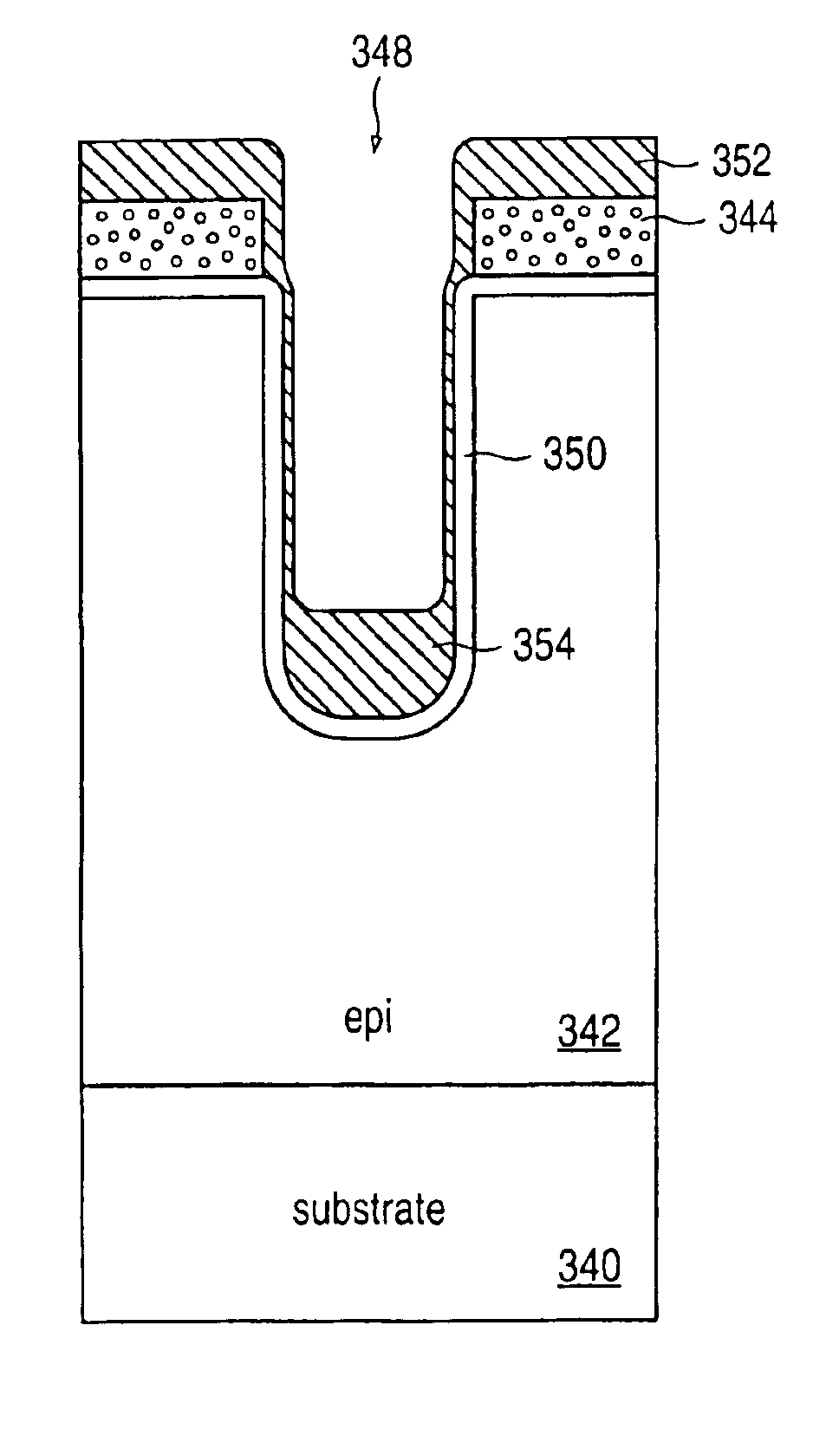
[0095]The problems associated with interactions between the gate and the drain of a MOSFET can be solved in part by reducing the coupling capacitance between them. In accordance with this invention, this is done by thickening the gate oxide layer at the bottom of the trench. FIGS. 11-27 show various structures and sequences for forming a thick gate oxide on the bottom of the trench.

[0096]FIG. 11A shows an epitaxial (“epi”) layer 242 grown on a substrate 240. A trench 250 is formed in epi layer 242. A gate oxide layer 244 lines the walls of trench 250, and a thick portion 246 of gate oxide layer 244 is located at the bottom of trench 250. Trench 250 is filled with polysilicon 248. Note that there is no oxide layer on top of polysilicon 248. The arrangement of FIG. 11A could be an intermediate structure; an oxide layer could be formed on top of polysilicon 248 at a later stage of the process. Polysilicon 248 is typically doped to a heavy doping concentration. It may be formed with a t...


PUM


Abstract

The a trench semiconductor device such as a power MOSFET the high electric field at the corner of the trench is diminished by increasing the thickness of the gate oxide layer at the bottom of the trench. Several processes for manufacturing such devices are described. In one group of processes a directional deposition of silicon oxide is performed after the trench has been etched, yielding a thick oxide layer at the bottom of the trench. Any oxide which deposits on the walls of the trench is removed before a thin gate oxide layer is grown on the walls. The trench is then filled with polysilicon in or more stages. In a variation of the process a small amount of photoresist is deposited on the oxide at the bottom of the trench before the walls of the trench are etched. Alternatively, polysilicon can be deposited in the trench and etched back until only a portion remains at the bottom of the trench. The polysilicon is then oxidized and the trench is refilled with polysilicon. The processes can be combined, with a directional deposition of oxide being followed by a filling and oxidation of polysilicon. A process of forming a “keyhole” shaped gate electrode includes depositing polysilicon at the bottom of the trench, oxidizing the top surface of the polysilicon, etching the oxidized polysilicon, and filling the trench with polysilicon.

Description

[0001]This application is a continuation of application Ser. No. 09 / 792,667, filed Feb. 21, 2001, now abandoned, which was a continuation of application Ser. No. 09 / 318,403, filed May 25, 1999, now U.S. Pat. No. 6,291,298. Each of the foregoing applications is incorporated herein by reference in its entirety.FIELD OF THE INVENTION[0002]This invention relates to semiconductor devices having a gate electrode that is embedded in a trench and in particular to structures and methods of protecting such devices against damage to the gate oxide layer when the devices are subjected to high voltage differences while in an off condition. The invention particularly relates to trench MOSFETs.BACKGROUND OF THE INVENTION[0003]There is a class of semiconductor devices in which a gate electrode is formed in a trench that extends from the surface of a semiconductor chip. One example is a trench-gated MOSFET, and other examples include insulated gate bipolar transistors (IGBTs), junction field-effect ...

Claims


Application Information

Patent Timeline
Patent Type & Authority Patents(United States)
IPC IPC(8): H01L21/02H01L21/336H01L29/78H01L29/66H01L29/08H01L29/10H01L29/423H01L29/02H01L29/40H01L21/76H01L21/8242
CPCH01L29/0878H01L29/42368H01L29/7828H01L29/7808H01L29/7811H01L29/7813H01L29/66734H01L29/0847H01L29/1095H01L29/4232H01L29/4238H01L29/7397H01L29/8083H01L21/762
Inventor WILLIAMS, RICHARD K.GRABOWSKI, WAYNE B.
Owner ADVANCED ANALOGIC TECHNOLOGIES INCORPORATED
Why Eureka
Try Eureka