Method and apparatus for inspecting a pattern formed on a substrate

a substrate and pattern technology, applied in the field of pattern inspection, can solve the problems of reducing the scheme of subject scanning with a spot-focused laser beam cannot be adopted, and the physical limit of high na-based design, so as to improve the contrast of the pattern

Inactive Publication Date: 2005-05-31
HITACHI HIGH-TECH CORP
View PDF11 Cites 38 Cited by
  • Summary
  • Abstract
  • Description
  • Claims
  • Application Information

AI Technical Summary

Benefits of technology

[0012]Means of alleviating the creation of speckles caused by the UV light according to this invention is a diffusion plate, and there is provided a means of moving the plate relative to the light beam in the direction virtually normal to the optical axis. In addition, with the intention of improving the contrast of pattern, it is devised, based on the fact that the polarization state of laser light can be manipulated, to be able to detect partially-polarized light components by controlling the direction of polarization of illumination light and the elliptic factor.

Problems solved by technology

However, the high NA based design is already at a physical limit, and the breakthrough approach is to shorten the wavelength of imaging light into the ranges of UV (ultraviolet) wavelengths of 300-380 nm, DUV (deep ultraviolet) wavelengths of 190-300 nm, VUV (vacuum ultraviolet) wavelengths of 100-190 nm, and EUV (extreme ultraviolet) wavelengths of the order of 10 nm.
Due to the requirement of high-speed inspection, the scheme of subject scanning with a spot-focused laser beam cannot be adopted.
Illumination of subject with a wide full-field laser light creates speckles, which cause overshooting and undershooting called “wringing” at edge of circuit pattern, resulting in a degraded image quality.

Method used


Image

  • Method and apparatus for inspecting a pattern formed on a substrate
  • Method and apparatus for inspecting a pattern formed on a substrate
  • Method and apparatus for inspecting a pattern formed on a substrate

Examples


Embodiment Construction

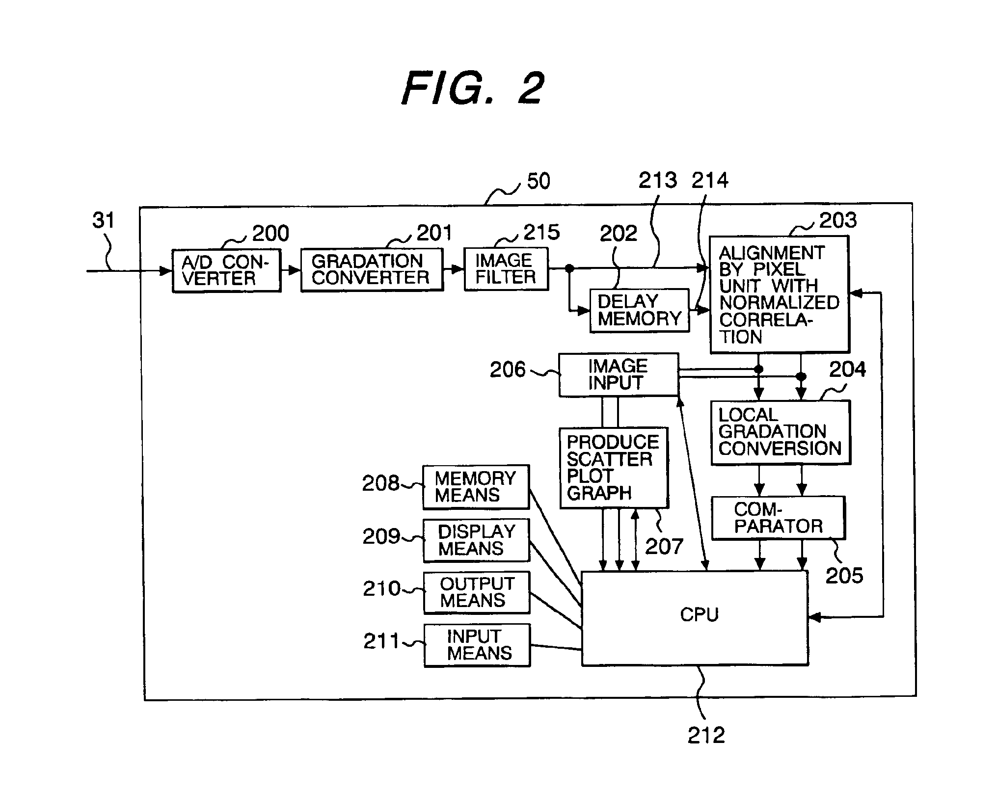
[0054]The method and apparatus for pattern defect inspection based on embodiments of this invention will be explained with reference to the drawings.

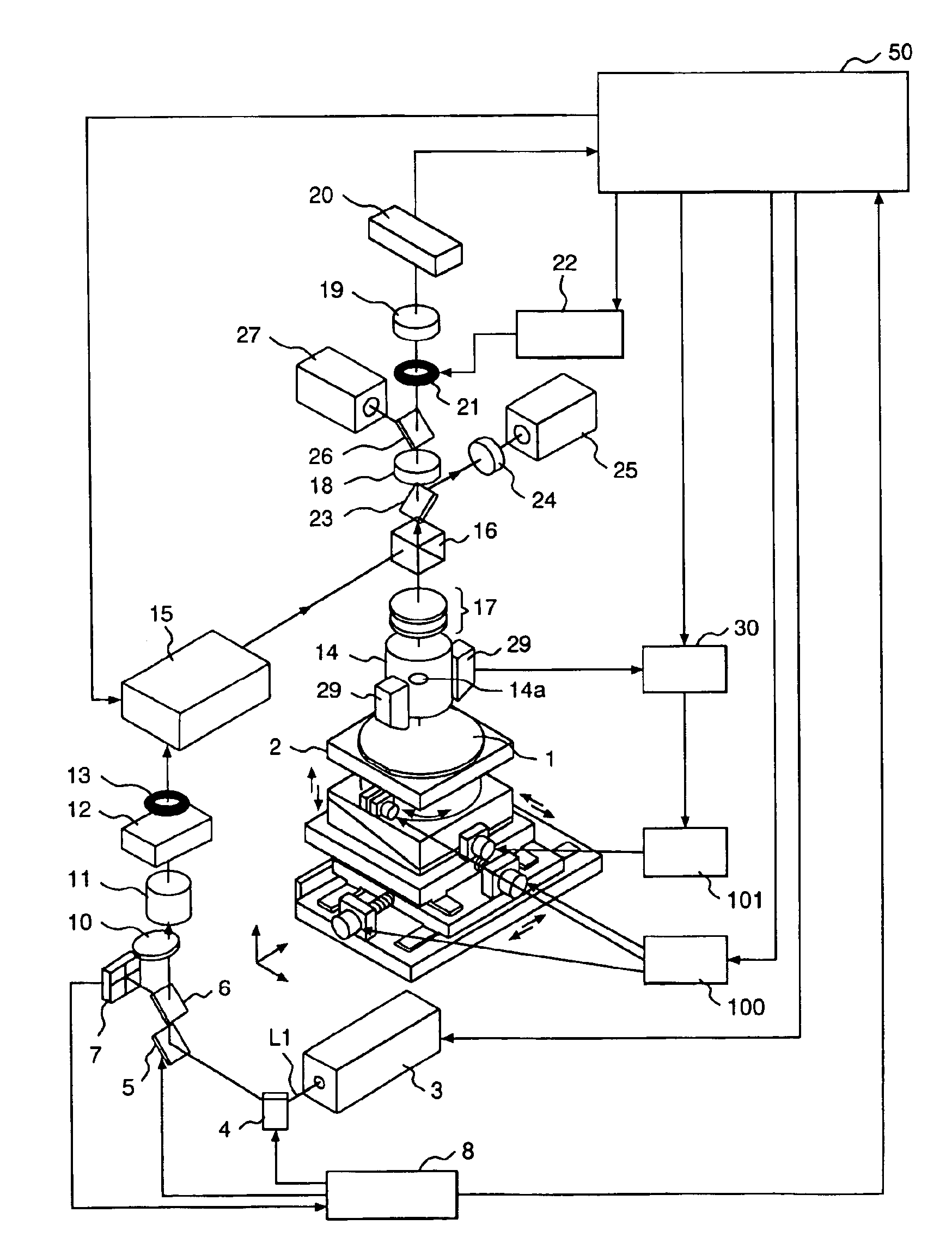
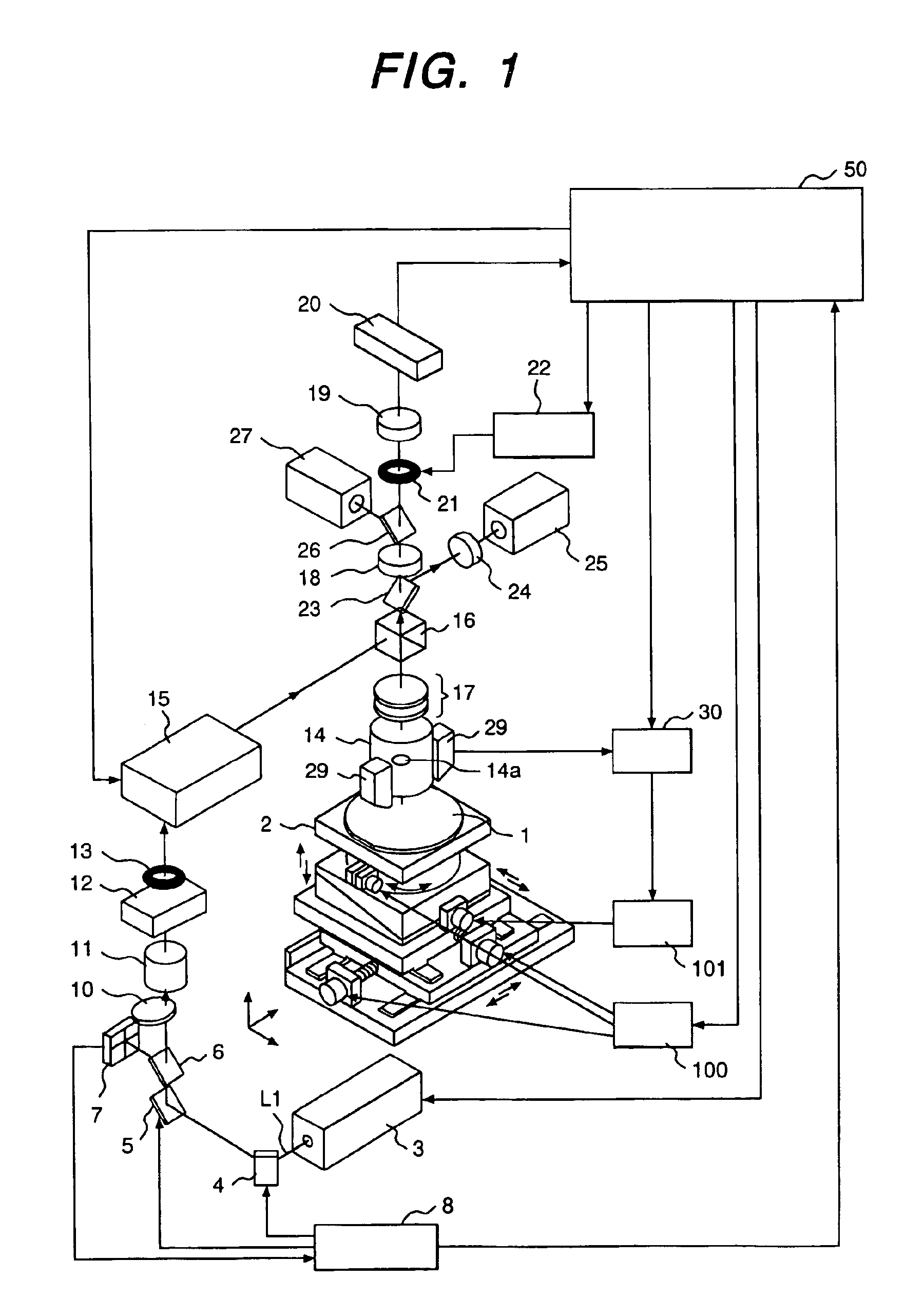
[0055]FIG. 1 shows an apparatus based on an embodiment of this invention. The apparatus includes a stage 2, which is made up of X, Y, Z and θ (rotation) stages, on which a semiconductor wafer (subject) 1 having a pattern to be inspected is placed. The X, Y and θ stages are operated by a drive circuit 100. The Z stage is operated by another drive circuit 101. An illumination light source 3 which illuminates the subject 1 consists of a UV laser source having a wavelength of 266 nm or 355 nm for example. The UV laser source is a device which implements the wavelength conversion for the solid YAG laser with nonlinear optical crystal, etc. to produce the third harmonic (355 nm) or fourth harmonic (266 nm) of the fundamental wave. A laser light source having a wavelength of 193 nm or 248 nm may be used alternatively. Using a laser source havi...


PUM

PropertyMeasurementUnit
diameteraaaaaaaaaa
sizeaaaaaaaaaa
wavelengthaaaaaaaaaa

Abstract

The inventive method and apparatus for detecting defects of a microscopic circuit pattern by imaging the pattern at high resolution comprises an objective lens for imaging the subject pattern, a laser illumination means for illuminating the pupil of the objective lens, means of diminishing the coherency of the laser illumination, an accumulative detector, and means of processing the signal detected by the detector. The method and apparatus are capable of imaging the subject pattern at high sensitivity and high speed based on the illumination by a short wavelength, which is indispensable for the enhancement of resolution, particularly based on a laser light source which is advantageous for practicing, with a resulting image being the same or better in quality as compared with an image resulting from the ordinary discharge tube illumination, whereby it is possible to detect microscopic defects at high sensitivity.

Description

CROSS REFERENCE TO RELATED APPLICATION[0001]This application is a continuation-in-part of U.S. application Ser. No. 10 / 218,463, filed Aug. 15, 2002, the subject matter of which is incorporated by reference herein.BACKGROUND OF THE INVENTION[0002]The present invention relates to the inspection of pattern for detecting defects (short-circuits, line breakages, etc.) and foreign particle on a pattern under test, and particularly to a method and apparatus of pattern inspection for detecting defects and foreign particle on a pattern of semiconductor wafer, liquid crystal display panel, photomask, etc. In the following explanation, the term “defect” is used to signify also foreign particle inclusively.[0003]There is a conventional pattern defect inspection apparatus which is designed to image a pattern under test with an imaging device such as a line sensor, while moving the pattern, and compare the image signal in terms of tone levels with the image signal which has been delayed by a pres...

Claims


Application Information

Patent Timeline
Patent Type & Authority Patents(United States)
IPC IPC(8): G01N21/956G01N21/88G03F7/20G03F9/00
CPCG03F7/7065G01N21/95684
Inventor YOSHIDA, MINORUMAEDA, SHUNJISHIMODA, ATSUSHISAKAI, KAORUOKABE, TAKAFUMIWATANABE, MASAHIRO
Owner HITACHI HIGH-TECH CORP
Why Eureka
Try Eureka