Semiconductor integrated circuit and its design methodology

Active Publication Date: 2005-06-14
RENESAS ELECTRONICS CORP
View PDF5 Cites 22 Cited by
  • Summary
  • Abstract
  • Description
  • Claims
  • Application Information

AI Technical Summary

Benefits of technology

[0018]Such an semiconductor integrated circuit apparatus can be implemented by arranging a logic circuit and a test control circuit; performing a clock tree synthesis for the logic circuit and the test control circuit; calculating a first delay of a clock signal supplied to flip-flops of the logic circuit and a second delay of a clock signal supplied to a pattern generation circuit of the test control circuit; and rewiring clock routing to the patt

Problems solved by technology

Since a scan operation consumes power for the entire circuit several times more than that consumed for normal operations, an excess voltage drop may cause incorrect detection of faults, or heat generation may cause chips to be damaged.
As logic circuits are designed for larger scales and higher performances, however, delays DSE1 and DSE2 of the scan enable signal and delays DCK1 and DCK2 of the clock signal become considerably larger than a clock cycle T. This is because progress towards the large-scale integration increases the number of FFs to be driven

Method used


Image

  • Semiconductor integrated circuit and its design methodology
  • Semiconductor integrated circuit and its design methodology
  • Semiconductor integrated circuit and its design methodology

Examples


Embodiment Construction

[0033]An invention for an integrated circuit that applies logic BIST at speed for large-scale and high-performance logic circuits without increasing test time is disclosed. Numerous specific details are set forth in order to provide a thorough understanding of the present invention. It will be understood, however, to one skilled in the art, that the present invention may be practiced without some or all of these specific details.

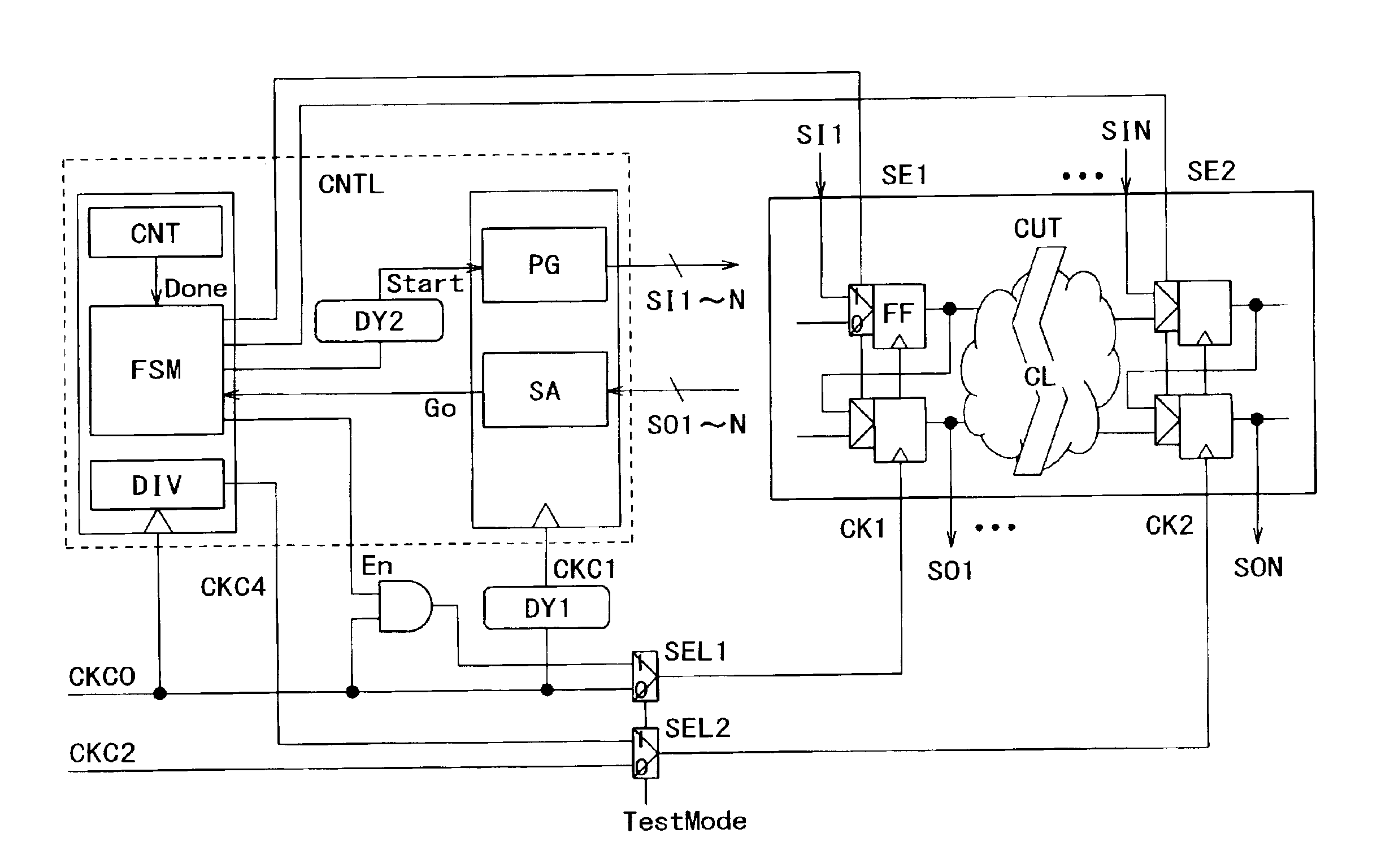
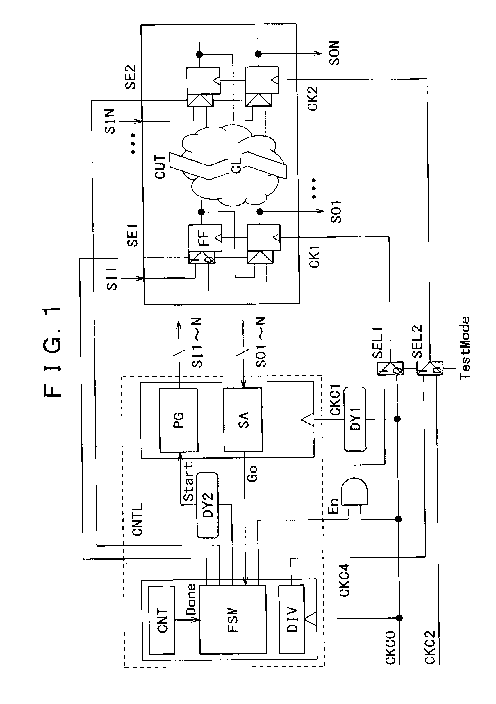
[0034]FIG. 1 is a circuit configuration diagram showing a semiconductor integrated circuit, in accordance with one embodiment of the present invention. In this example, a user circuit CUT is supplied with clock signals CK1 and CK2 having different frequencies. A scan enable signal SE1 is supplied to a flip-flop operating in synchronization with a clock signal CK1. A scan enable signal SE2 is supplied to a flip-flop operating in synchronization with a clock signal CK2. When the user circuit CUT is supplied with clock signals having k types of frequencies diff...


PUM


Abstract

A method and device are provided for applying logic BIST at speed for large-scale and high-performance logic circuits without increasing test time, and decreasing test costs as a result. In one example, a logic BIST controller is divided into two portions. A clock signal having a small delay is used to drive a partial circuit that supplies a user circuit with a scan enable signal and a clock signal. A clock signal having a large delay is used to drive a partial circuit that supplies the user circuit with a test pattern and collects a test result.

Description

BACKGROUND OF THE INVENTION[0001]1. Field of the Invention[0002]The present invention generally relates to a semiconductor integrated circuit and, more particularly, to a semiconductor integrated circuit having a logic circuit including storage elements.[0003]2. Discussion of Background[0004]Logic BIST (Built-In Self Test) has become to be widely used in order to avoid increasing tester investments resulting from availability of large-scale and high-performance logic circuits. Logic BIST uses a fault-detecting logic BIST controller installed on a semiconductor integrated circuit chip and enables testing at the same operating frequency (i.e., “at speed”) as for normal operations even on a low-cost tester having low operating frequencies.[0005]Processes of applying logic BIST to logic circuits will be described with reference to the accompanying drawings. FIG. 11 (PRIOR ART) is a circuit configuration diagram showing a conventional logic BIST controller. A configuration of a conventio...

Claims


Application Information

Patent Timeline
IPC IPC(8): G01R31/28G01R31/3185G01R31/3183G06F11/22G06F17/50H01L21/82H01L21/822H01L27/04H03K5/135H03K19/00H03K19/173
CPCG01R31/318594G01R31/318552
Inventor KOHNO, ICHIRO
Owner RENESAS ELECTRONICS CORP
Why Eureka
Try Eureka