Semiconductor device and method for fabricating such device

a technology of semiconductor devices and dielectric layers, applied in the direction of semiconductor devices, electrical equipment, transistors, etc., can solve the problems of inability to increase drain current as desired, difficulty in photolithography, and other problems, to achieve the effect of preventing the breakdown of the gate dielectric layer, and stable operation characteristics

Inactive Publication Date: 2005-06-28
RICOH KK
View PDF8 Cites 113 Cited by
  • Summary
  • Abstract
  • Description
  • Claims
  • Application Information

AI Technical Summary

Benefits of technology

[0058]In addition, in the first exemplary embodiment (1), with the bipolar transistor turned on, when a potential is applied to the emitter and gate electrode, the voltage created between the base and the emitter is only a forward-biased voltage. A high voltage does not appear at the gate electrode of the transistor. Accordingly, the breakdown of the gate dielectric layer can be prevented even when a high voltage (i.e., the source potential) is applied. Therefore, stable operational characteristics is obtained for a bipolar transistor.
[0059]In the

Problems solved by technology

Also, in the structure of FIG. 8B, another difficulty may arise during photolithography and etching process steps for forming the gate oxide 104a.
In these structures of FIGS. 8B and 8C, therefore, difficulties arise in implementing the miniaturization of the transistors.
As a result, there arises a difficulty in the previous channel type LDMOS transistor, in that drain current cannot be increased as desired with the increase in the gate voltage, as illustrated in FIG.
In addition, there encountered is another difficulty as illustrated in FIG. 12A, in which a drain breakdown is caused with relative ease after parasitic bipolar operations in the high voltage range for MOS transistor drain.
In this structure, however, a source of the transistor is not formed in the self-aligned manner, thereby resulting in remaining source resistance.
As a result, there remains some source resistance, which is insufficient for reducing the on resistance of the transistor.
This is therefore indicative of a still persisting difficulty of lo

Method used


Image

  • Semiconductor device and method for fabricating such device
  • Semiconductor device and method for fabricating such device
  • Semiconductor device and method for fabricating such device

Examples


examples

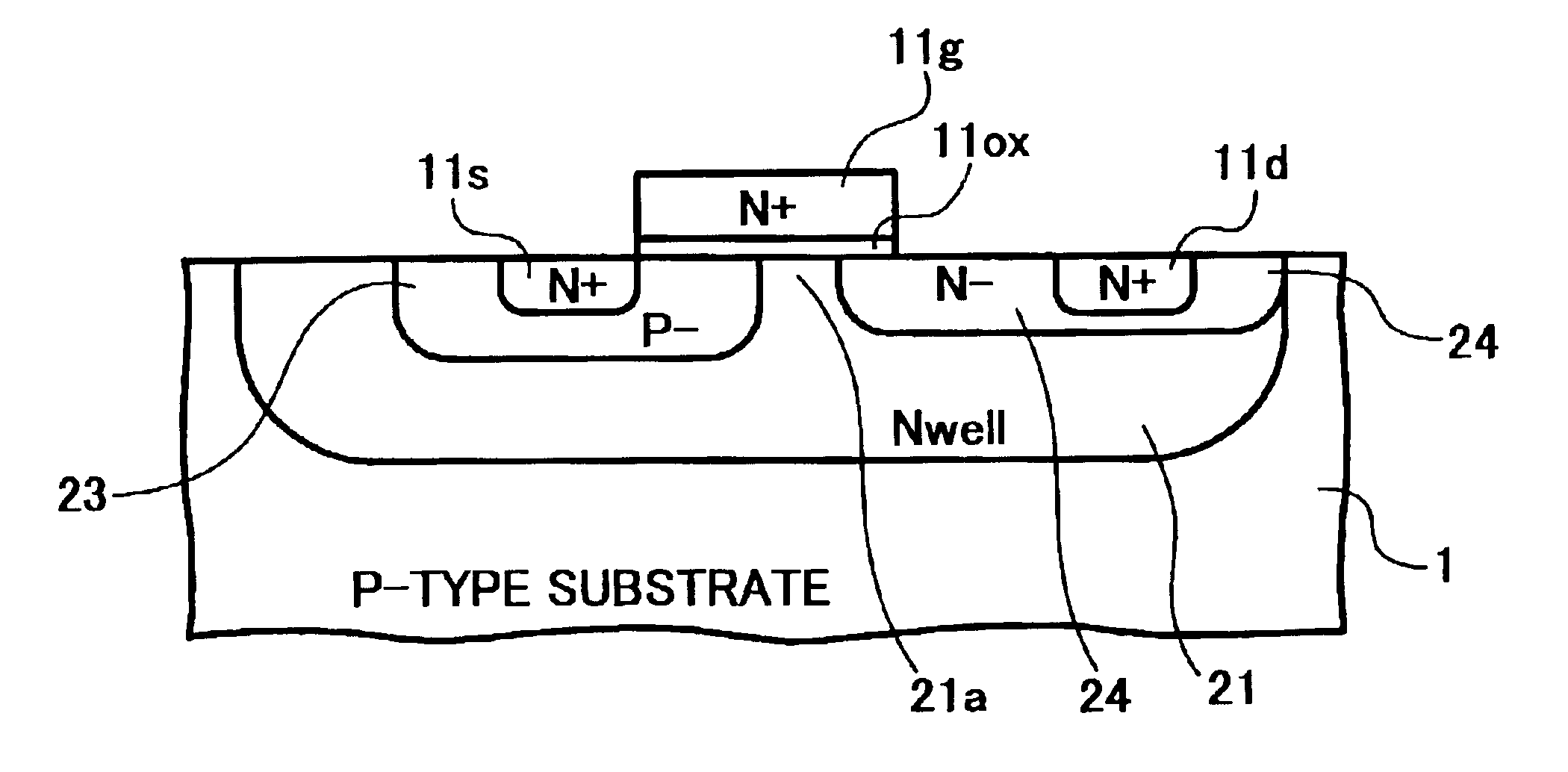
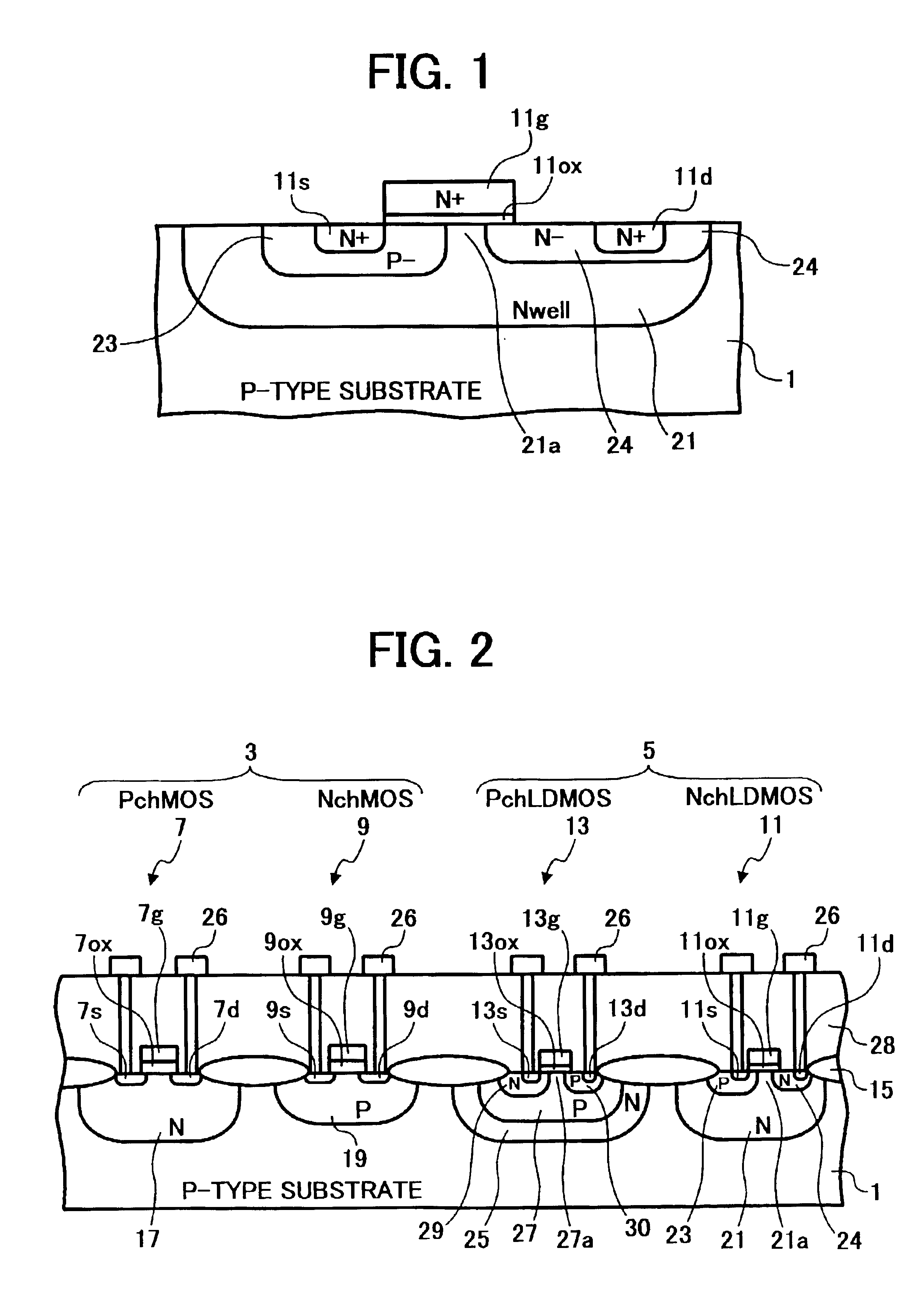
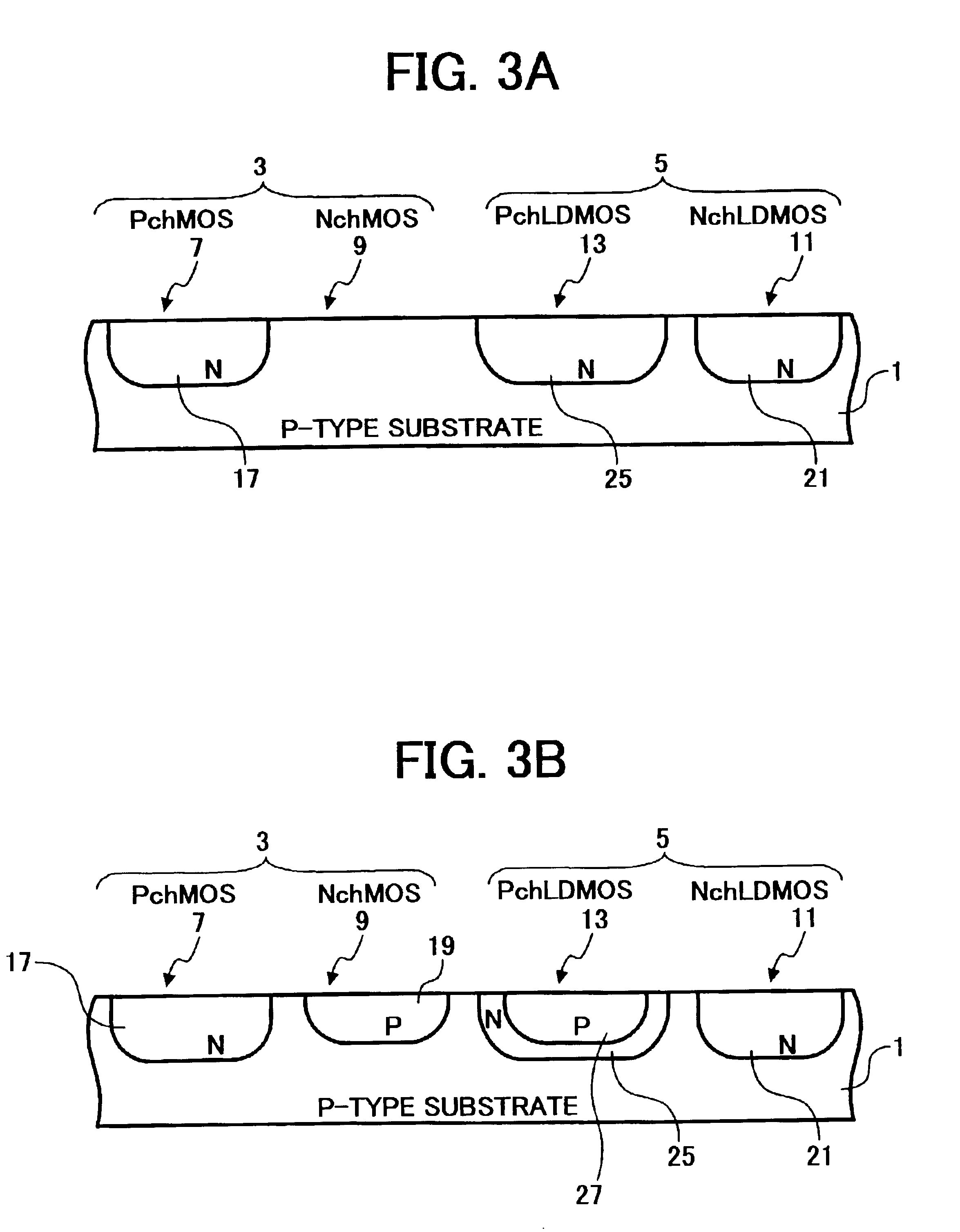
[0143]FIG. 1 is a diagrammatic cross-sectional view illustrating an NchLDMOS transistor according one embodiment disclosed herein.

[0144]Referring to FIG. 1, an N-type drain well region 21 is formed in a P-type substrate 1.

[0145]In the N-type drain well region 21, a P-type well region 23 is subsequently formed, a portion of which serves as a channel region. In addition, an N-type source 11s is formed in the P-type well region 23.

[0146]Also formed in the N-type well region 21 is a medium concentration N-type drain region 24, which is spatially separated from the P-type well region 23 having a concentration of N-type impurities such as, for example, phosphorous ions higher than that of the N-type well region 21.

[0147]Furthermore, an N-type drain 11d is formed in the medium concentration N-type drain region 24 having another concentration of N-type impurities such as, for example, phosphorous ions higher than that of the medium concentration N-type drain region 24.

[0148]An N-type gate e...


PUM


Abstract

An LDMOS transistor and a bipolar transistor with LDMOS structures are disclosed for suitable use in high withstand voltage device applications, among others. The LDMOS transistor includes a drain well region 21 formed in P-type substrate 1, and also formed therein spatially separated one another are a channel well region 23 and a medium concentration drain region 24 having an impurity concentration larger than that of drain well region 21, which are simultaneously formed having a large diffusion depth through thermal processing. A source 11s is formed in channel well region 23, while a drain 11d is formed in drain region 24 having an impurity concentration larger than that of drain region 24. In addition, a gate electrode 11g is formed over the well region, overlying the partially overlapped portions with well region 23 and drain region 24 and being separated from drain 11d. Since the source 11s, well region 23, and drain region 24 are respectively self-aligned to the gate electrode 11g, resultant transistor characteristics are stabilized, and the decrease in the on resistance and improved drain threshold voltages can be achieved. Also disclosed herein are bipolar transistors with LDMOS structures, which are capable of obviating the breakdown of gate dielectric layers even at high applied voltage and achieving improved stability in transistor characteristics.

Description

FIELD OF THE INVENTION[0001]This patent specification relates generally to a semiconductor device and methods for fabricating such device, and more specifically to a semiconductor device incorporating either an LDMOS transistor or a bipolar transistor with LDMOS structure, for suitable use in device applications with high withstand voltage.BACKGROUND OF THE INVENTION[0002]As the use of semiconductor devices incorporating regulator and DC / DC converter circuits becomes more widespread, it is increasingly important to meet the demands for higher output currents of these devices among others.[0003]In one approach to achieve the high output currents, LDMOS transistors have been attracting much attention, which operate with low on resistance. In addition, the LDMOS transistors are known to have a structure suitable for miniaturization with a decreased chip area yet attaining high withstand voltages.[0004]The “LDMOS (lateral double-diffusion MOS) transistor” is a field effect transistor, i...

Claims


Application Information

Patent Timeline
IPC IPC(8): H01L29/732H01L29/78H01L21/70H01L29/735H01L29/66H01L21/8238H01L27/085H01L27/092H01L29/08H01L29/02
CPCH01L21/823857H01L21/823892H01L27/0922H01L27/0928H01L29/7835H01L29/66674H01L29/66681H01L29/7322H01L29/735H01L29/7801H01L29/7816H01L29/0847H01L29/0878H01L29/1083H01L29/4238
Inventor NEGORO, TAKAAKIFUJIMOTO, KEIJI
Owner RICOH KK
Why Eureka
Try Eureka