

Film thickness measuring method, relative dielectric constant measuring method, film thickness measuring apparatus, and relative dielectric constant measuring apparatus
a film thickness and measuring method technology, applied in the direction of mechanical measuring arrangements, semiconductor/solid-state device testing/measurement, instruments, etc., can solve the problems of mercury being detrimental to the human body, method is not desirable, optical method cannot always achieve accurate measurement, etc., to achieve the effect of accurately measuring the thickness of an insulator film
- Summary
- Abstract
- Description
- Claims
- Application Information
AI Technical Summary
Benefits of technology
Problems solved by technology
Method used
Image

Examples
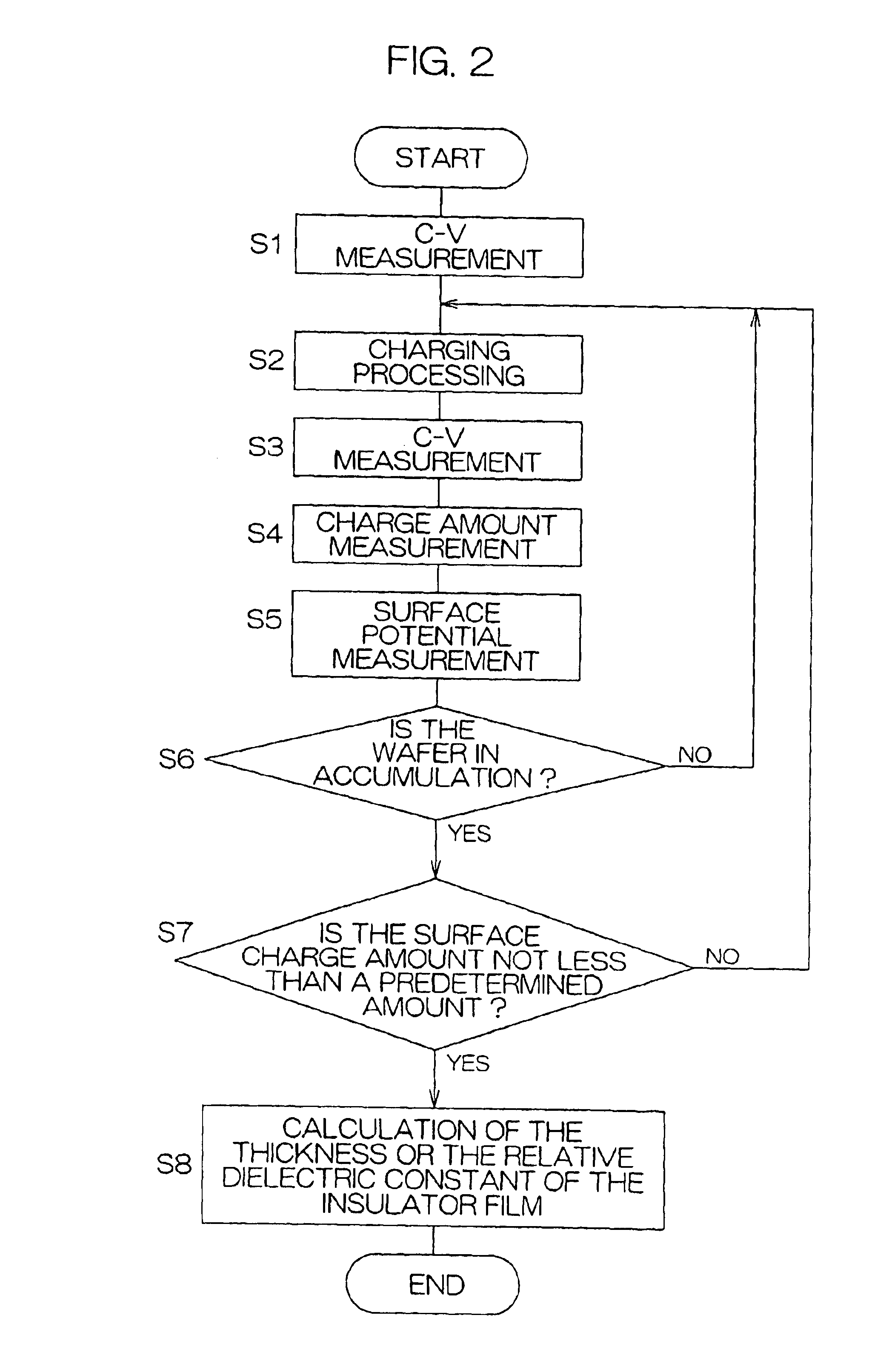
first embodiment
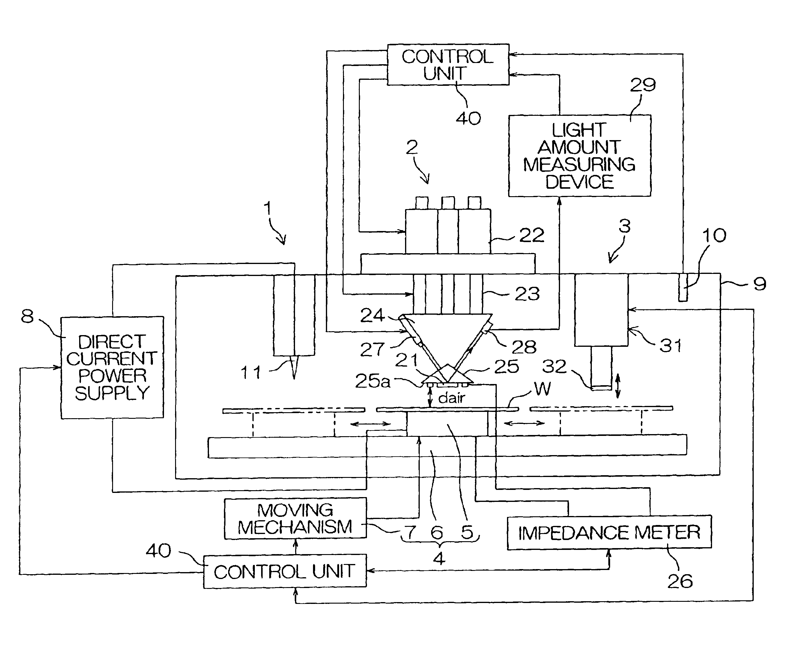
[0053]FIG. 1 is a schematic front view of a thickness / relative dielectric constant measuring apparatus according to the present invention.
[0054]This thickness / relative dielectric constant measuring apparatus is arranged to measure the thickness or relative dielectric constant of an insulator film formed on a surface of a wafer W as an example of a semiconductor substrate, and comprises a chamber 9. The apparatus further comprises a charging processing unit 1, a charge amount measuring unit 2 and a surface potential measuring unit 3 which are arranged to execute a processing or measurement in the chamber 9. The charging processing unit 1, the charge amount measuring unit 2 and the surface potential measuring unit 3 are successively linearly disposed. The wafer W is arranged to be moved, by a loader 4, among a charging processing position at the charging processing unit 1, a C-V measuring position at the charge amount measuring unit 2, and a surface potential measuring position at the...
second embodiment
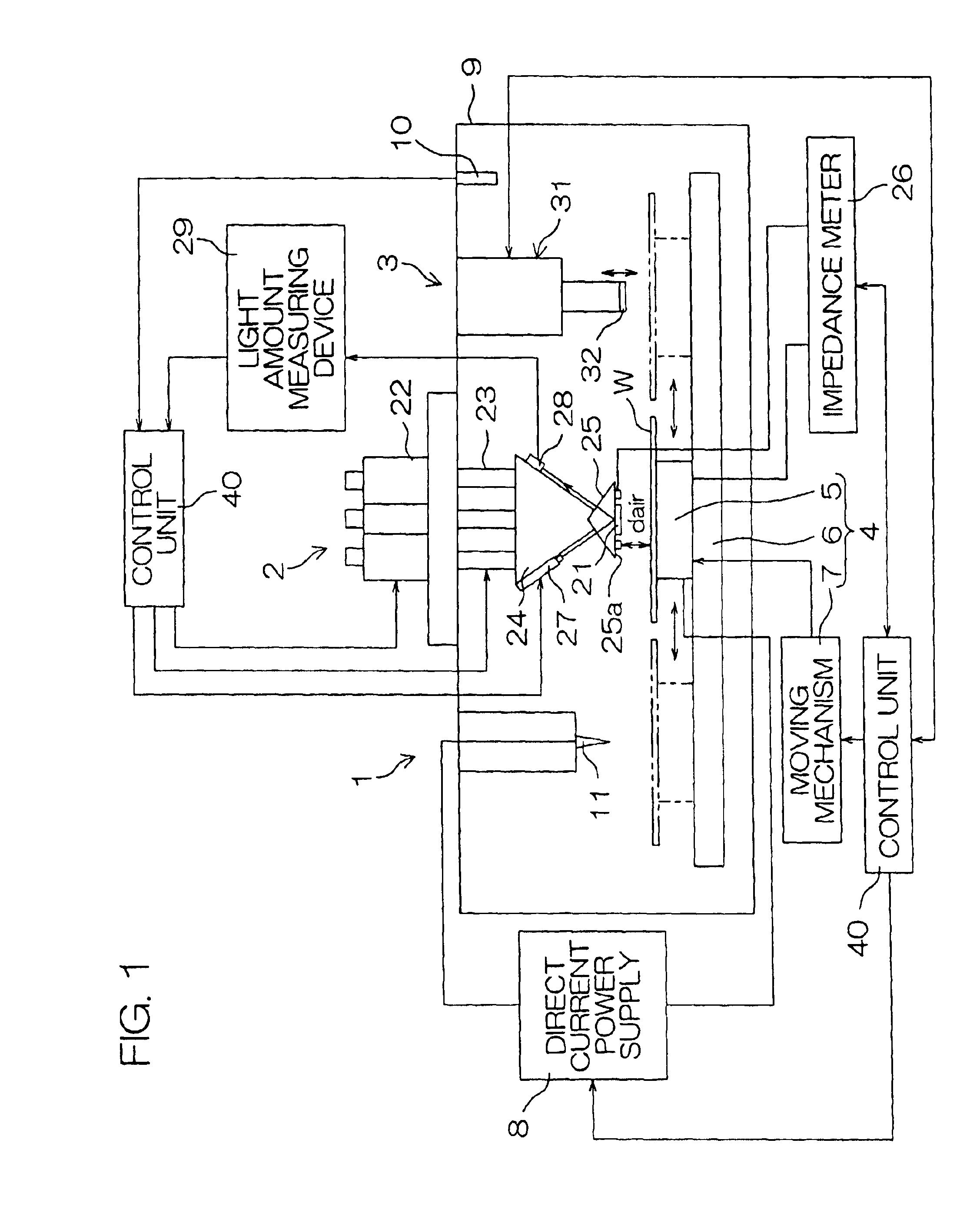
[0101]FIG. 5 is a schematic front view of a film thickness / relative dielectric constant measuring apparatus according to the present invention. In FIG. 5, like parts are generally designated by like reference numerals used in FIG. 1.
[0102]This film thickness / relative dielectric constant measuring apparatus 50 comprises, as a charging processing unit, an ultraviolet ray (UV) irradiation unit 41, instead of the charging processing unit 1 having the needle 11 in the film thickness / relative dielectric constant measuring apparatus 20 in FIG. 1. The ultraviolet ray irradiation unit 41 comprises an ultraviolet ray lamp 42 and an optical system 43. The ultraviolet ray lamp 42 is arranged to receive an electric power supplied from a lamp power source 48 and to generate ultraviolet rays having a wavelength of, for example, not less than 220 nm and not greater than 300 nm. The operation of the lamp power source 48 is controlled by a control unit 40.
[0103]The optical system 43 comprises a mirro...
PUM
| Property | Measurement | Unit |
|---|---|---|
| wavelength | aaaaa | aaaaa |
| wavelength | aaaaa | aaaaa |
| thickness/relative dielectric constant | aaaaa | aaaaa |
Abstract
Description
Claims
Application Information