Organic electroluminescent device and display unit
- Summary
- Abstract
- Description
- Claims
- Application Information
AI Technical Summary
Benefits of technology
Problems solved by technology
Method used
Image
Examples
example 1
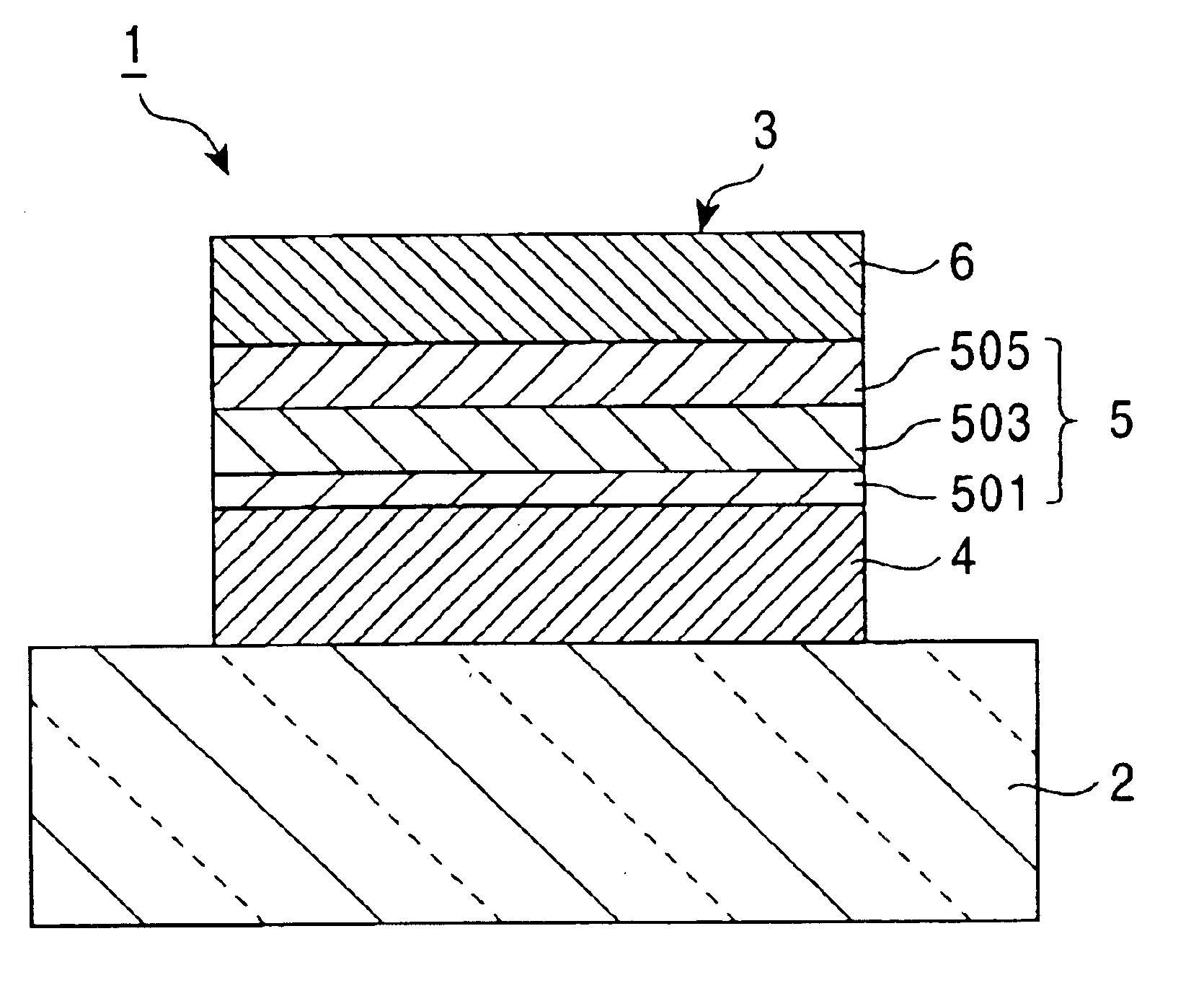
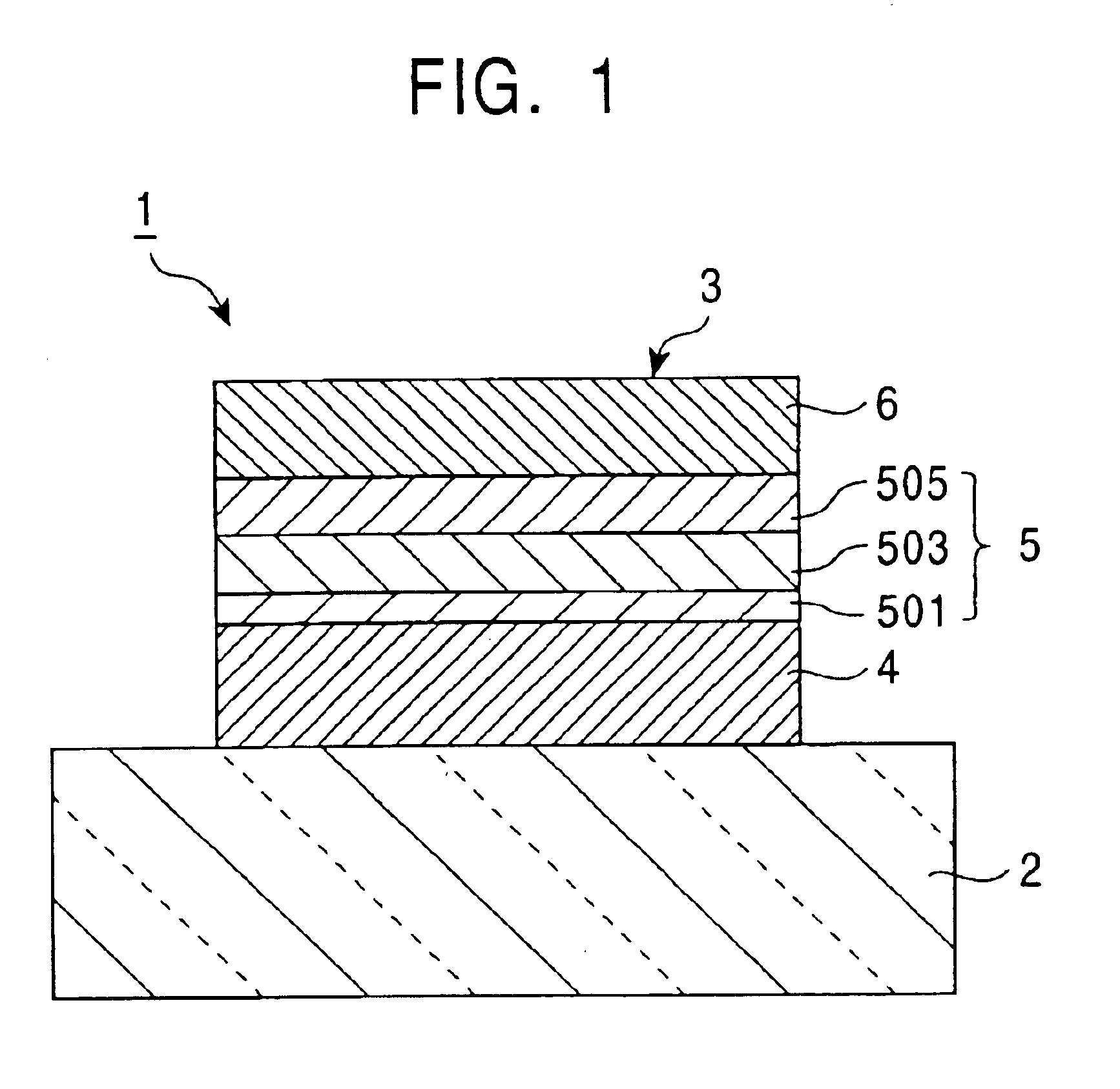
[0074]Each of layers (1) to (6) having respective film thicknesses as described below was formed on a glass substrate in that order and, therefore, an organic electroluminescent device to become a blue-emitting element was produced. At that time, an anode material (1) was made into a film by sputtering, and thereafter, an insulation film (silicon oxide film) having an opening window for exposing the anode material within the range of 2 mm×2 mm was formed on the substrate. Layers from a hole injection layer (2) to buffer layer (5) were formed on the anode material (1) by vacuum deposition from above a vapor deposition mask. Subsequently, the vapor deposition mask was removed, and a cathode material (6) was laminated on the buffer layer (5) by vacuum deposition.[0075](1) anode: ITO 190 nm,[0076](2) hole injection layer: 2-TNATA [4,4′,4″-tris(2-naphthylphenylamino)triphenylamine] 20 nm,[0077](3) hole transportation layer: triphenylamine tetramer represented by the aforementioned Struct...
example 2
[0082]An organic electroluminescent device was produced in a manner similar to that in Example 1 except that the hole transportation layer (3) shown in Example 1 was formed using triphenylamine tetramer represented by the aforementioned Structural formula (3) where R31 to R36=H with a film thickness of 50 nm.
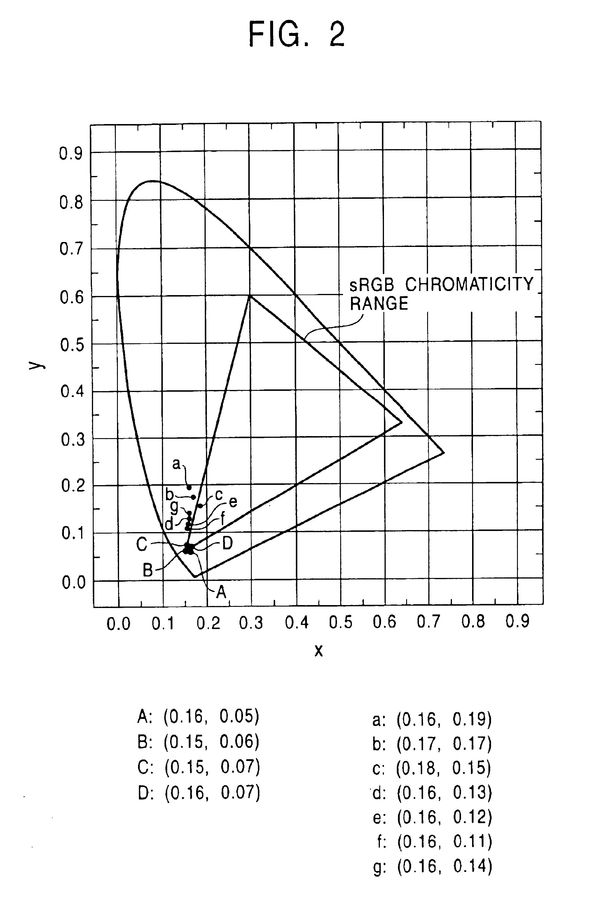
[0083]The characteristics of the organic electroluminescent device produced as described above were measured. As a result, the coordinate on the CIE chromaticity coordinates was B(0.15, 0.06) indicated by the point B in the chromaticity diagram shown in FIG. 2, and it was confirmed that the high purity blue emission very close to the blue chromaticity (0.14, 0.07) based on the NTSC standard and blue chromaticity (0.15, 0.06) based on the sRGB could be achieved. As shown in FIG. 4, the emission spectrum had intense peaks at 446 nm and 426 nm, and the full width at half maximum of these peaks was 60 nm. Furthermore, the brightness at a current density of 25 mA / cm2 was 242 cd / m2 an...
example 3
[0086]Each of layers (1) to (7) having respective film thicknesses as described below was formed on a glass substrate in that order and, therefore, an organic electroluminescent device to become a blue-emitting element was produced. At that time, an anode material (1) was made into a film by sputtering, and thereafter, an insulation film (silicon oxide film) having an opening window for exposing the anode material within the range of 2 mm×2 mm was formed on the substrate. Layers from a hole injection layer (2) to buffer layer (6) were formed on the anode material (1) by vacuum deposition from above a vapor deposition mask. Subsequently, the vapor deposition mask was removed, and a cathode material (7) was laminated on the buffer layer material (6) by vacuum deposition.[0087](1) anode: ITO 190 nm,[0088](2) hole injection layer: 2-TNATA [4,4′,4″-tris(2-naphthylphenylamino)triphenylamine] 20 nm,[0089](3) hole transportation layer: triphenylamine tetramer represented by the aforemention...
PUM
| Property | Measurement | Unit |
|---|---|---|
| Purity | aaaaa | aaaaa |
| Light | aaaaa | aaaaa |
| Luminescence | aaaaa | aaaaa |
Abstract
Description
Claims
Application Information


