Charge pump circuit and PLL circuit using same

a pump circuit and circuit technology, applied in pulse automatic control, dc-dc conversion, power conversion systems, etc., can solve the problems of large current consumption, large current consumption, and inability to solve large current consumption, so as to improve the stability of the oscillation frequency of the vco, large drivability, and high precision

Active Publication Date: 2005-07-19
SONY SEMICON SOLUTIONS CORP
View PDF6 Cites 27 Cited by
  • Summary
  • Abstract
  • Description
  • Claims
  • Application Information

AI Technical Summary

Benefits of technology

[0019]An object of the present invention is to provide a charge pump circuit able to enhance the rising and falling characteristics of the current output, drive the current output with a short pulse, reduce the leakage current at the OFF time of not outputting the current, and realize a reduction of the power consumption and a PLL circuit using the same.
[0029]Further, when switching the second or third transistor in accordance with the up signal or the down signal, by appropriately controlling the timing of the control signal, by turning off the third transistor earlier than the second transistor being turned on, and by turning on the third transistor later than the second transistor being turned off, the second and third transistors being simultaneously on can be avoided, the release or injection of charge current from or to the output terminal of the charge pump circuit can be prevented, and the stability of the oscillation frequency of the VCO can be improved.
[0030]Further, by controlling the timing of the charge current and the discharge current output by the charge pump circuit by the lock signal supplied to the first transistor, a large drivability can be secured, the rising and falling edges of the output current can be sharply controlled, and therefore it is possible to control the oscillation frequency of the VCO with a high precision.

Problems solved by technology

Due to this, the leakage current at the OFF time of the transistor tends to increase.
However, the current IDX and IUP flow through the transistors NT3 and PT3 also at the OFF time, so there is a problem of a large current consumption.
In the charge pump circuit shown in FIG. 9, however, the current IDN and the current IUP flow through the transistors NT3 and PT3 also at the OFF time, so the problem of large current consumption is not solved.
Further, a buffer amplifier AMP1 requiring an output larger than the current IDN and the current IUP is necessary, so there are problems in that the power consumption further increases and the size of the circuit becomes large.
In general, it is difficult to raise this drive signal sharply.
Further, this drive signal is not a logic signal, but an analog signal also needing amplitude information, so a buffer circuit of a logic able to easily raise the drivability cannot be used.
Note that, in the charge pump circuit shown in FIG. 8, not only at the nMOS transistor side for generating the discharge current IDN, but also at the pMOS transistor side for generating the charge current IUP, similarly, the drive signal supplied to the gate of the transistor PT2 is an analog signal having amplitude information, so sharp rising is difficult due to the limitation of the drivability.
Due to the above reasons, the rising characteristic of the drive signal supplied to the gate of the transistor NT2 is poor, so it becomes impossible to drive this by a pulse signal having a short width.
For this reason, in the PLL circuit connected to the output terminal OUT of the charge pump circuit, receiving the output current of the charge pump circuit, generating a control signal SC, and controlling the oscillation frequency of the voltage control oscillator (VCO) by using this control signal SC, there are the disadvantages that the precision of the control signal SC is lowered and it becomes impossible to control the oscillation frequency with a high precision.

Method used


Image

  • Charge pump circuit and PLL circuit using same
  • Charge pump circuit and PLL circuit using same
  • Charge pump circuit and PLL circuit using same

Examples


first embodiment

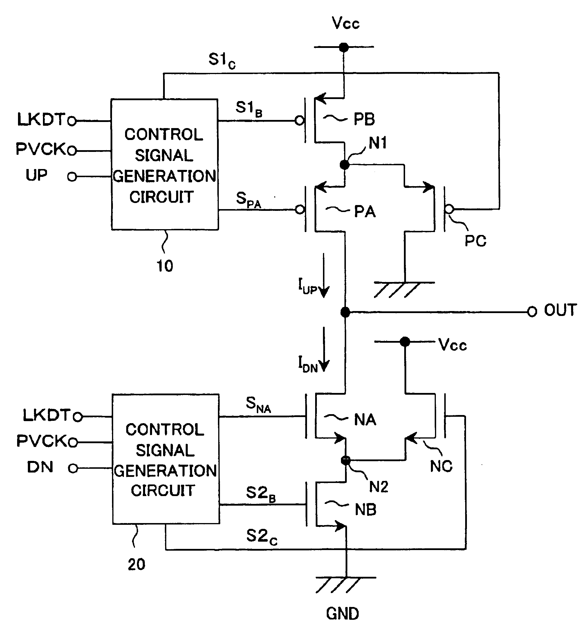
[0042]FIG. 1 is a circuit diagram of a first embodiment of a charge pump circuit according to the present invention.

[0043]As illustrated, the charge pump circuit of the present embodiment is configured by nMOS transistors NA, NB, and NC, pMOS transistors PA, PB, and PC, and control signal generation circuits 10 and 20.

[0044]The transistors PB and PA are connected in series between a terminal of the power supply voltage VCC and an output terminal OUT of the charge pump circuit. Namely, the source of the transistor PB is connected to the terminal supplied with the power supply voltage VCC, and the drain is connected to a source of the transistor PA. The drain of the transistor PA is connected to the output terminal OUT. The source of the transistor PC is connected to a connection point N1 between the drain of the transistor PB and the source of the transistor PA, and the drain is grounded.

[0045]The gate of the transistor PA is supplied with an analog control signal SPA output by the c...

second embodiment

[0110]FIG. 6 is a circuit diagram of a second embodiment of a charge pump circuit according to the present invention.

[0111]As illustrated, the charge pump circuit of the present embodiment is configured by control signal generation circuits 10A and 20A, pMOS transistors PA, PB, and PD, and nMOS transistors NA, NB and ND.

[0112]In comparison with the first embodiment of the charge pump circuit of the present invention shown in FIG. 1, in the charge pump circuit of the present embodiment, an nMOS transistor ND is used in place of the pMOS transistor PC, and a PMOS transistor PD is used in place of the nMOS transistor NC.

[0113]As shown in FIG. 6, in the transistor ND, the drain is connected to the connection point N1 of the drain of the transistor PB and the source of the transistor PA, and the source is grounded. The gate of the transistor ND is supplied with the control signal S1D output by the control signal generation circuit 10A.

[0114]On the other hand, in the transistor PD, the so...

third embodiment

[0120]FIG. 7 is a view of the configuration of an embodiment of a PLL circuit according to the present invention.

[0121]As illustrated, the PLL circuit of the present embodiment comprises a phase frequency comparison circuit 100, a lock detection circuit 110, a charge pump circuit 120, a loop filter 130, a VCO 140, and a frequency divider 150.

[0122]Below, an explanation will be given of the components of the PLL circuit of the present embodiment.

[0123]The phase frequency comparison circuit 100 compares the phases and frequencies of a reference clock signal RCK and the frequency divided clock signal VCK output from the frequency divider 150 and, as a result of the comparison, outputs the up signal UP or the down signal DN in accordance with the phase difference between the reference clock signal RCK and the frequency divided clock signal VCK.

[0124]The lock detection circuit 110 detects whether or not the PLL circuit is in the locked state in accordance with the up signal UP and the do...


PUM


Abstract

A charge pump circuit able to enhance the rising and falling characteristics of a current output, drive the current output with a short pulse, reduce leakage current at the OFF time when a current is not output, and realize a reduction of a power consumption and a PLL circuit using same. By outputting a charge current or a discharge current in accordance with an up signal or a down signal and turning on a third transistor (PC, NC) at the OFF time when the current is not output, an inverse bias voltage is supplied between a gate and a source of the second transistor (PA, NA), whereby a reduction of the leakage current can be realized. When the second or third transistor is switched in accordance with the up signal or the down signal, the timing of the control signal is appropriately controlled, simultaneous turning on of the second and third transistors can be avoided, release or injection of charges from and to the output terminal of the charge pump circuit can be prevented, and the stability of an oscillation frequency of a VCO can be improved.

Description

BACKGROUND OF THE INVENTION[0001]1. Field of the Invention[0002]The present invention relates to a charge pump circuit and a phase locked loop (PLL) circuit using a charge pump circuit, for example a PLL circuit for generating local oscillation signals in a wireless communication system and a charge pump circuit used for that.[0003]2. Description of the Related Art[0004]When a charge pump circuit is off, leakage current induces a voltage fluctuation of an output signal of the charge pump circuit and has become one of the causes inducing fluctuation of the oscillation frequency of a PLL circuit. For this reason, a reduction of the leakage current at the OFF time is an important characteristic required for the charge pump circuit. In recent years, power supply voltage has been lowered along with miniaturization of a semiconductor device, so it becomes necessary to lower a threshold voltage of a transistor for operation at a low voltage. Due to this, the leakage current at the OFF time...

Claims


Application Information

Patent Timeline
Patent Type & Authority Patents(United States)
IPC IPC(8): H03L7/089H03L7/095H03L7/08H03L7/093
CPCH03L7/0891H03L7/095
Inventor SUZUKI, NORIHITO
Owner SONY SEMICON SOLUTIONS CORP
Why Eureka
Try Eureka