Nanopastes as patterning compositions for electronic parts

a technology of electronic parts and compositions, applied in the direction of photosensitive materials, instruments, circuit masks, etc., can solve the problem of surprising low viscosity of dispersion, and achieve the effect of substantially increasing the conductivity of the resulting pattern area

Inactive Publication Date: 2005-07-26
KODAK POLYCHROME GRAPHICS
View PDF26 Cites 53 Cited by
  • Summary
  • Abstract
  • Description
  • Claims
  • Application Information

AI Technical Summary

Benefits of technology

[0009]The inorganic nanoparticles may form a stable dispersion in the carrier at room temperature. Further, the inorganic nanoparticles are of such a size that the viscosity of the dispersion is surprisingly low. This property, in part, allows for a high concentration of inorganic nanoparticles to be included in the nanopaste without adversely affecting the application of the nanopaste to a substrate. In one embodiment, the inorganic nanoparticles compose between about 0.5 and about 75 w / w % of the nanopaste.

Problems solved by technology

Further, the inorganic nanoparticles are of such a size that the viscosity of the dispersion is surprisingly low.

Method used


Image

  • Nanopastes as patterning compositions for electronic parts
  • Nanopastes as patterning compositions for electronic parts
  • Nanopastes as patterning compositions for electronic parts

Examples


example 1

Ink-Jet Formation of a Printed Circuit Board

[0044]A sample of Nema FR4 N4000-2, an epoxy laminate available from New England Laminates Ltd, Skelmersdale, UK and composed of woven borosilicate glass fiber yarn, was modified so as to be free of copper layers. This was accomplished by immersing the laminate in a CuCl2 stripping solution, which was composed of water (100 kg), anhydrous copper chloride (40 kg), and HCl (60 kg of a 28 w / w % solution)), at 60° C. until the copper was removed. The remaining laminate was then washed with water and dried.

[0045]The resulting substrate was then placed on the platten of a JetPlate printer (available from Pisces-Print Imaging Sciences Inc., Nashua, N.H.) and a conductive pattern area was then produced by patternwise ink-jet application of Ag / Pd sol, a nanopaste having a metallic particle mean diameter of 11.1, supplied as a 5 w / w % solution in water and available from ANP. The pattern area was dried, and then the electrical conductivity of the pa...

example 2

Formation of an Electronic Part

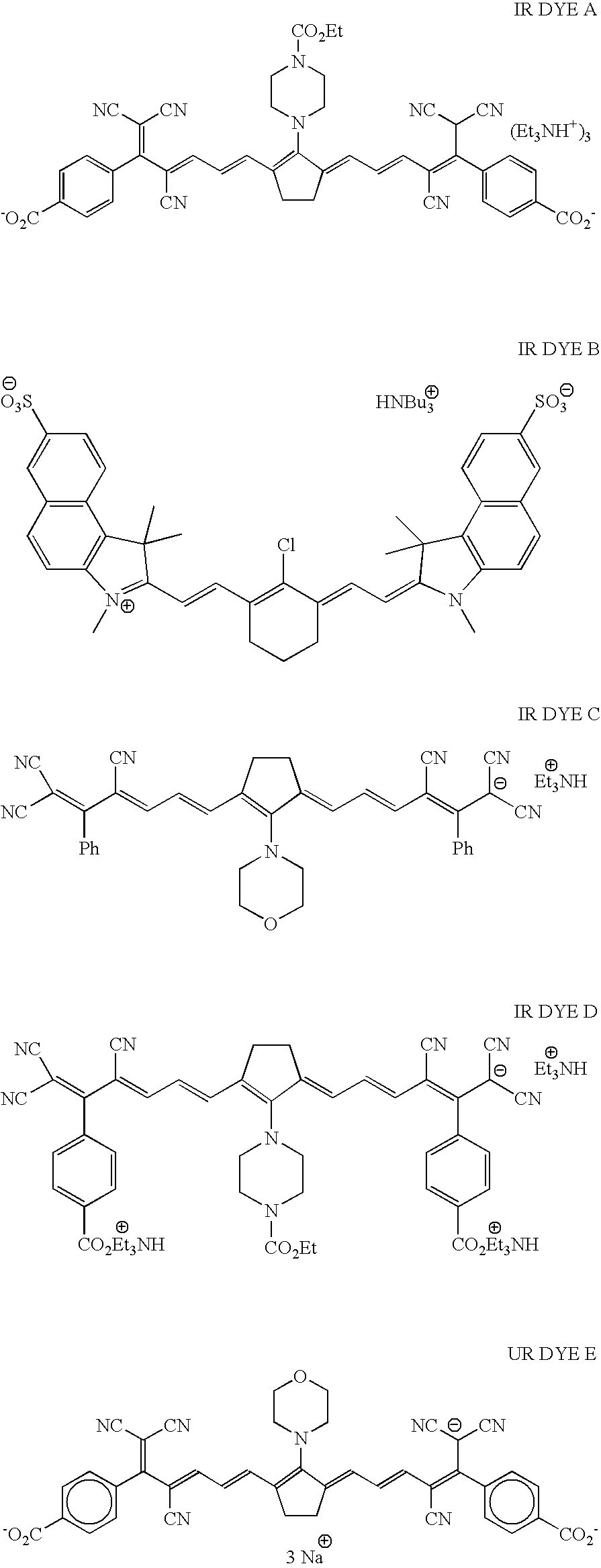
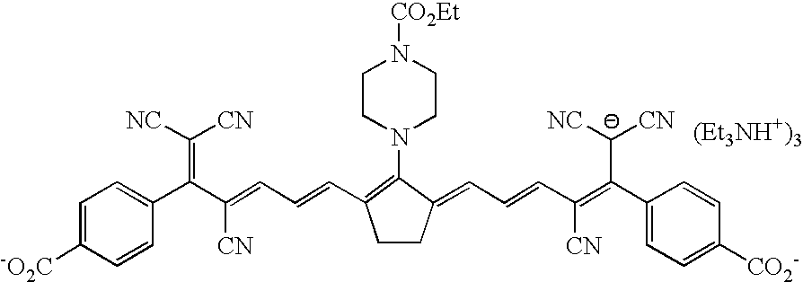
[0047]A sample of Nema FR4 N4000-2 is modified as in Example 1 so as to be free of copper layers. The resulting substrate is coated via a wire wound bar with a layer of a thermally sensitive composition composed of Ag sol (90 w / w %) and IR dye A (10 w / w %). Ag sol is an inorganic nanopaste having a metallic particle mean diameter of 11.0 nm in a 5 w / w % solution in water, which is available from ANP, Korea. IR dye A is represented by the following structure:

[0048]A sample of the resulting plate precursor is then patternwise exposed at 195 mJ / cm2 using an internal test pattern on a Creo Trendsetter 3230, a placesetter operating at a wavelength of 830 nm and available from Creo Products Inc., Burnaby, BC, Canada. Exposure results in a color change from gray to copper-like. The sample is then immersed for 20 seconds in 956 developer, a phenoxyethanol based developer available from Kodak Polychrome Graphics, Norwalk Conn. The non-exposed areas are washed ...


PUM

PropertyMeasurementUnit
diameteraaaaaaaaaa
diameteraaaaaaaaaa
diameteraaaaaaaaaa

Abstract

The present invention provides methods of making an electronic part in which a nanopaste composed of inorganic nanoparticles and a carrier is applied onto a surface of a substrate. The composition is then processed to form an electrically conductive pattern area that adheres to the surface of the substrate. Optionally, the conductivity of the pattern area may be improved by heating.

Description

BACKGROUND OF THE INVENTION[0001]Printed circuit boards and other electronic parts generally include electrically conductive patterns or tracks formed on a non-conductive surface of a substrate. The electrically conductive patterns are traditionally formed by selectively applying an etchant to a layer of conductive material applied onto the non-conductive surface of the substrate. Portions of the conductive layer that contact the etchant are removed to reveal the surface of the substrate, and portions of the conductive layer that are not contacted by the etchant remain in the form of the desired conductive pattern. Selective application of the etchant is normally accomplished by placing an etch resistant mask over the conductive layer such that only those portions of the conductive material intended to form the conductive patterns are covered with the etch resistant mask. During etching, revealed portions of the conductive layer are removed, while portions covered with the mask rema...

Claims


Application Information

Patent Timeline
Patent Type & Authority Patents(United States)
IPC IPC(8): H05K3/02H05K3/12H05K3/00H05K1/09G03F7/004
CPCH05K3/02H05K3/125H05K3/1283G03F7/0047H05K1/095H05K3/0082H05K2201/0257H05K2203/013H05K2203/0514H05K2203/1105Y10S430/145Y10S430/165
Inventor RAY, KEVIN BARRYSHIMAZU, KEN-ICHIKITSON, ANTHONY PAUL
Owner KODAK POLYCHROME GRAPHICS
Why Eureka
Try Eureka