CAM circuit with radiation resistance

a cam circuit and radiation resistance technology, applied in the field of low-power cam arrays, can solve the problems of significantly more power, noise generation, and significant power needed (and generated) in the cam array, and achieve the effect of reducing the chance of “soft error” discharge and increasing the cost and power consumption of the cam circui

Inactive Publication Date: 2005-08-02
AVAGO TECH WIRELESS IP SINGAPORE PTE
View PDF14 Cites 4 Cited by
  • Summary
  • Abstract
  • Description
  • Claims
  • Application Information

AI Technical Summary

Benefits of technology

[0011]The present invention is directed to a CAM circuit that addresses the soft error problem associated with the low power CAM operating environment by providing a doped layer below both the logic and memory portions of each C

Problems solved by technology

Therefore, a relatively small portion of the entire RAM array circuitry is activated at one time to perform each data word read/write operation, so a relatively small amount of switching noise occurs within the RAM array, and the amount of power required to operate the RAM array is relatively small.
While CAM arrays are faster than RAM arrays in performing search functions, they consume significantly more power and generate significantly more switching noise than RAM arrays.
In particular, in contrast to RAM arrays in which only a small portion of the total circuitry is accessed during each read and write operation, significantly more power is needed (and noise is generated) in a CAM array because, during compare (search) operations, all of the CAM cells are accessed simultaneously, and those CAM cells that do not match the applied search data value typically switch a

Method used


Image

  • CAM circuit with radiation resistance
  • CAM circuit with radiation resistance
  • CAM circuit with radiation resistance

Examples


Embodiment Construction

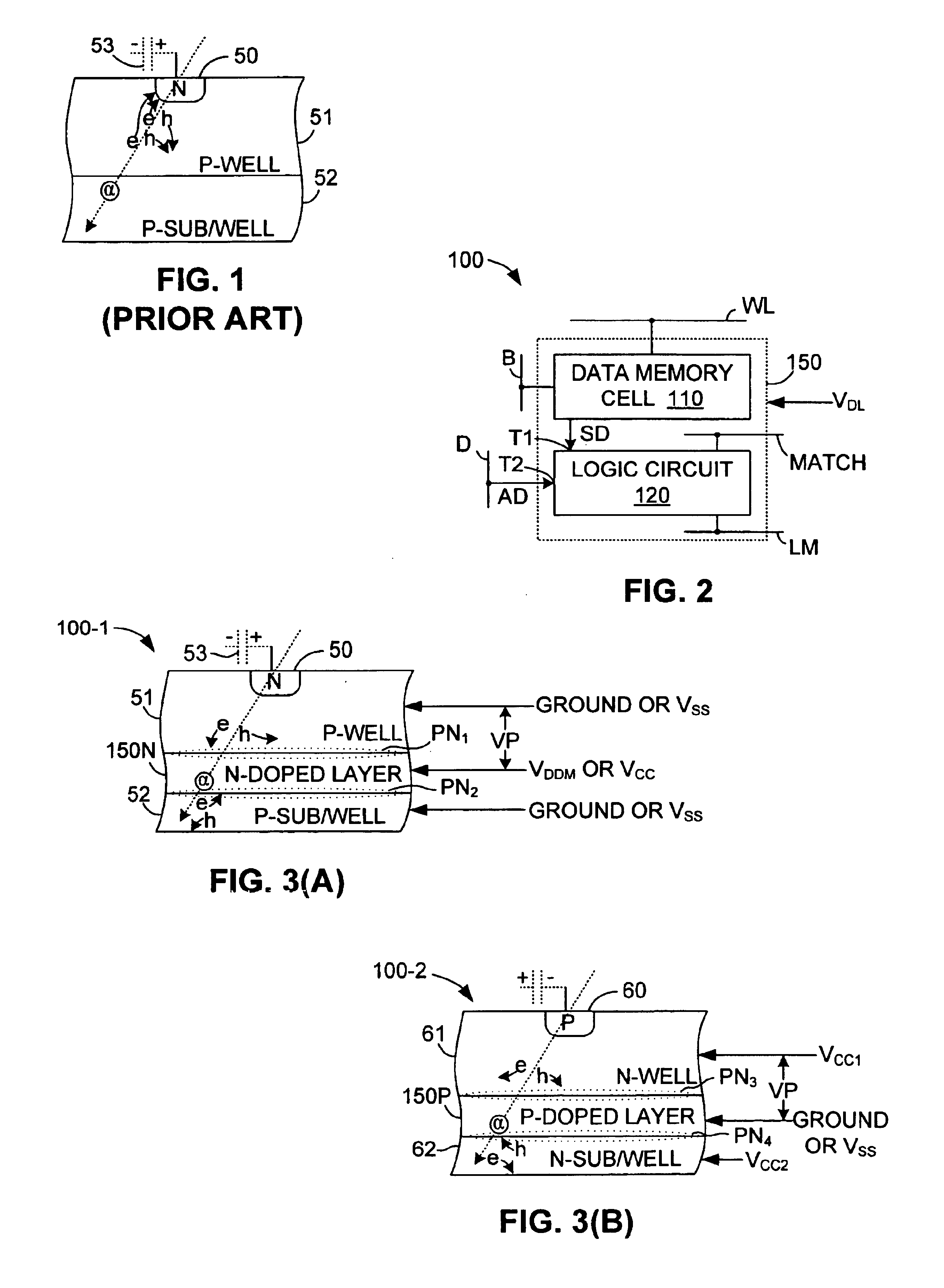
[0024]The present invention is described below with specific reference to binary SRAM CAM cells and ternary DRAM CAM cells. However, it is noted that the present invention can be extended to include other types of CAM cells, including ternary and quad (four-state) SRAM CAM cells, as well as binary DRAM CAM cells. Further, the specific CAM cell embodiments described herein are intended to be exemplary, and not limiting (unless otherwise specified in the claims).

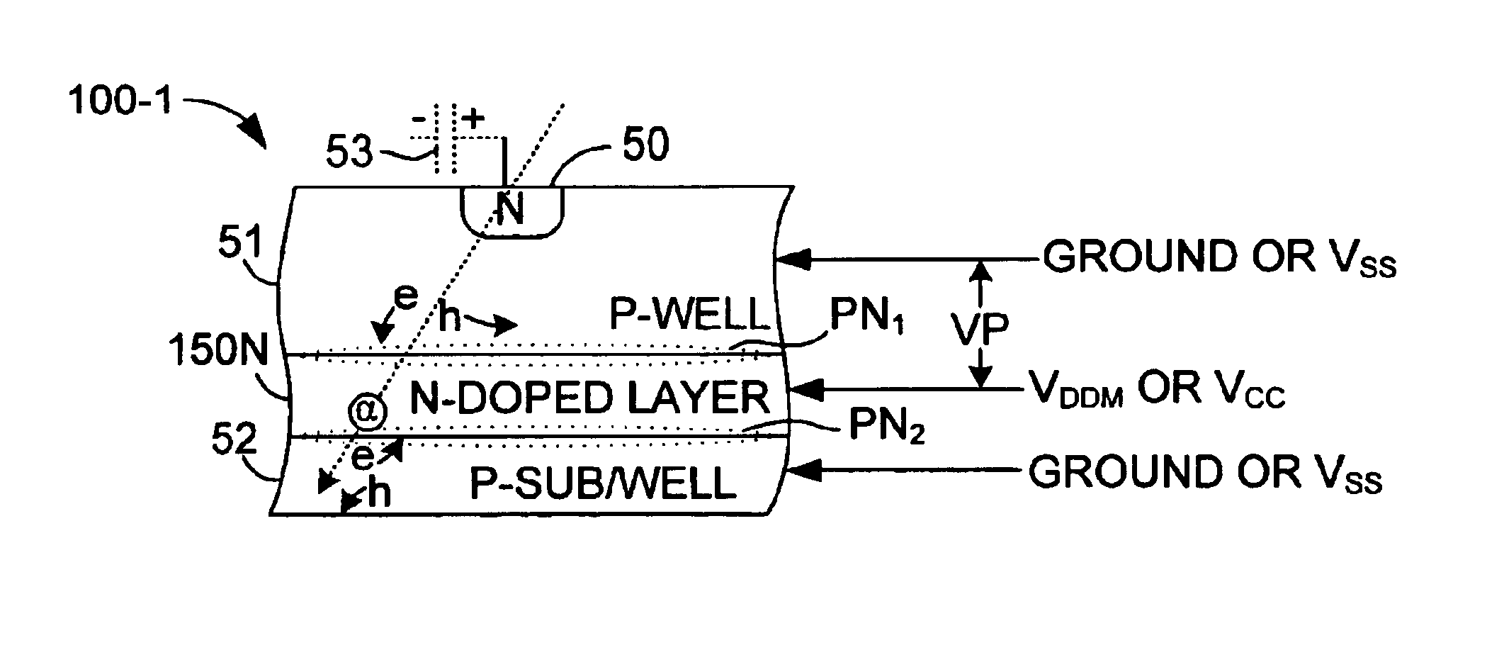
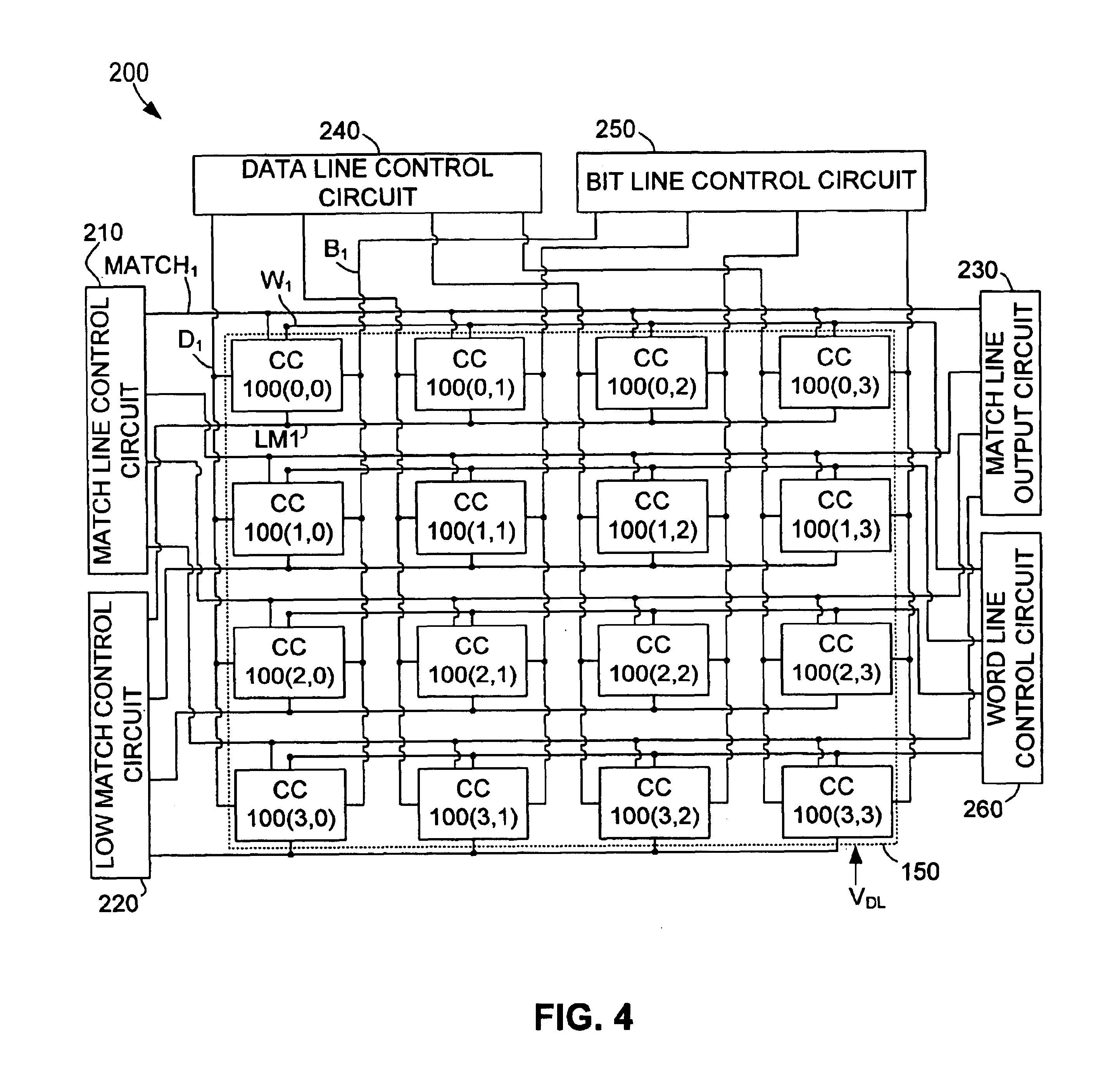
[0025]FIG. 2 is a block diagram showing a simplified CAM cell 100 in accordance with the present invention. CAM cell 100 includes a data memory cell 110 and a comparator (logic) circuit 120 that are fabricated using CMOS techniques. In one embodiment, both data memory cell 110 and comparator circuit 120 are formed using at least one n-channel transistor having an n-doped storage region (junctions) formed in a p-type well, which in turn is formed in a p-type substrate (or in a larger p-type region formed in an n-type substrate)...


PUM


Abstract

A CMOS CAM circuit an array of CAMs formed on a p-type substrate. Each CAM cell includes a logic portion and an SRAM cell, both having at least one n-channel transistor formed in a p-type well on the p-type substrate. An n-type doped layer is formed between the p-type well region and the p-substrate. The doped layer and well region are maintained at a voltage potential that is between a threshold voltage and a breakdown voltage defined the PN junction formed at their interface. The resulting structure attracts electron-hole pairs formed by alpha particles, thereby preventing soft errors. Alternatively, the logic portions and SRAM cells have p-channel transistors formed in n-type wells on an n-type substrate, and a p-type doped layer is formed between the n-type well region and the n-substrate.

Description

CROSS-REFERENCE TO RELATED APPLICATIONS[0001]The present application is a continuation-in-part of U.S. application Ser. No. 10 / 165,506, which was filed on Jun. 6, 2002 U.S. Pat. No. 6,754,093.FIELD OF THE INVENTION[0002]The present invention relates to integrated content addressable memory (CAM) arrays, and in particular to low-power CAM arrays.DISCUSSION OF RELATED ART[0003]Conventional random access memory (RAM) arrays include RAM cells (e.g., static RAM (SRAM) cells, dynamic RAM (DRAM) cells, and non-volatile RAM (NVRAM) cells) that are arranged in rows and columns, and addressing circuitry that accesses a selected row of RAM cells using address data corresponding to the physical address of the RAM cells within the RAM array. A data word is typically written into a RAM array by applying physical address signals to the RAM array input terminals to access a particular group of RAM cells, and applying data word signals to the RAM array input terminals that are written into the acces...

Claims


Application Information

Patent Timeline
IPC IPC(8): G11C15/00G11C15/04G11C5/00
CPCG11C5/005G11C15/04G11C15/043
Inventor LIEN, CHUEN-DER
Owner AVAGO TECH WIRELESS IP SINGAPORE PTE
Why Eureka
Try Eureka