Split poly-SiGe/poly-Si alloy gate stack

a poly-sige alloy and gate stack technology, applied in the direction of transistors, electrical devices, semiconductor devices, etc., can solve the problems of very difficult to adjust the thermal energy required for activation of dopant impurities, small and small gate electrodes, and a very thin gate insulating layer, etc., to achieve enhanced boron diffusion and boron activation, and good cosi2 formation

Inactive Publication Date: 2005-08-09
GLOBALFOUNDRIES U S INC
View PDF15 Cites 24 Cited by
  • Summary
  • Abstract
  • Description
  • Claims
  • Application Information

AI Technical Summary

Benefits of technology

[0011]It is a further object of the present invention to provide an improved FET device gate structure and process for so making.
[0013]It is yet another object of the present invention to provide a FET gate structure that is simple, easy to fabricate and provides reliable gate control.
[0014]It is still yet another object of the present invention to provide a simple gate structure that is effective to avoid the deleterious effects of the thermal energy required to be employed for FET device fabrication.
[0015]In accordance with the present invention, a simple process and material solution acts to allow the use of a single gate stack structure for both nFETs and pFETs and results in both n-gate and p-gate electrode stacks which are easily silicided and p-gate electrodes with high boron activation and, hence, little gate electrode depletion. This is achieved by employing an insitu Rapid Thermal Chemical Vapor Deposition (RTCVD) process for creating an effective SiGe polycrystalline multi-layer gate electrode structure.
[0017]The gate structure thus formed, in accordance with the present invention, is such that the nanocrystalline Si layer allows both continuity of RTCVD poly SiGe deposition even at high Ge concentrations and formation of small grain size. In turn, the small grain size of the nanocrystalline Si layer allows both enhanced boron diffusion and boron activation. The formation of a monolayer of SiO2, for example, on the poly-SiGe is sufficiently thin to readily permit current flow but yet is sufficient to block diffusion upwardly in the gate stack to the polysilicon layer so as to thereby allow good formation of CoSi2, particularly on nFET gate structures.

Problems solved by technology

The desire for increased speed and density, however, has resulted smaller and smaller gate electrodes and extremely thin gate insulating layers.
Although this solution is effective in overcoming the “short channel” effect problem, it has manifested at least one other problem in its effective implementation.
This problem is centered on the fact that the thermal energy required for activation of dopant impurity is very difficult to adjust.
As a result, this creates another short channel effect problem.
This creates gate electron depletion affecting, in turn, the integrity of the threshold of the gate.
However, it has been found that the high Ge concentration in the polysilicon results in very poor CoSi2 formation on the gate structures, and particularly on the nFET gate structures.
The poor CoSi2 formation has been attributed to the fact that the Ge diffusion coefficient in the SiGe alloy through poly-grain boundaries is extremely high.
Therefore, poly-silicide formation of the poly-SiGe alloy gate and metal cobalt is practically impossible since cobalt is unreactive chemically with the element Ge.
On the other hand, the element Ge is also known to have a high surface energy and, thus, the SiGe alloy material is extremely difficult to be made to chemically absorb on the gate dielectric structure of multi-layer polysilicon gate structures.
However, as Ge concentration is increased up to around 20% and above, SiGe alloy becomes discontinuous.

Method used


Image

  • Split poly-SiGe/poly-Si alloy gate stack
  • Split poly-SiGe/poly-Si alloy gate stack
  • Split poly-SiGe/poly-Si alloy gate stack

Examples


Embodiment Construction

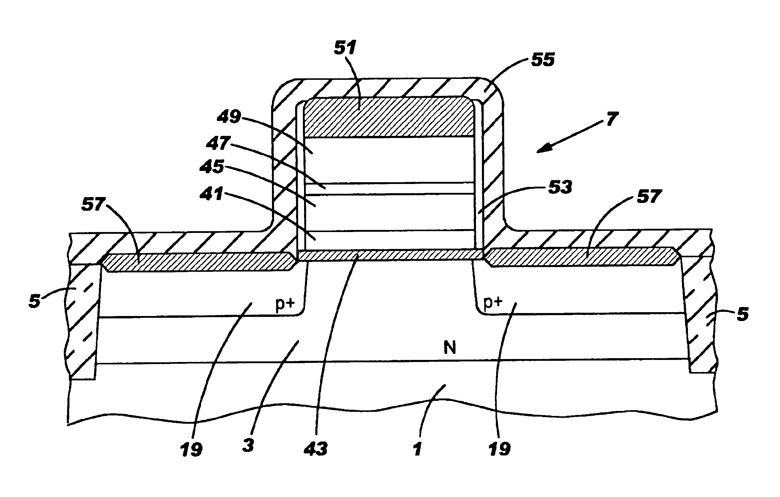
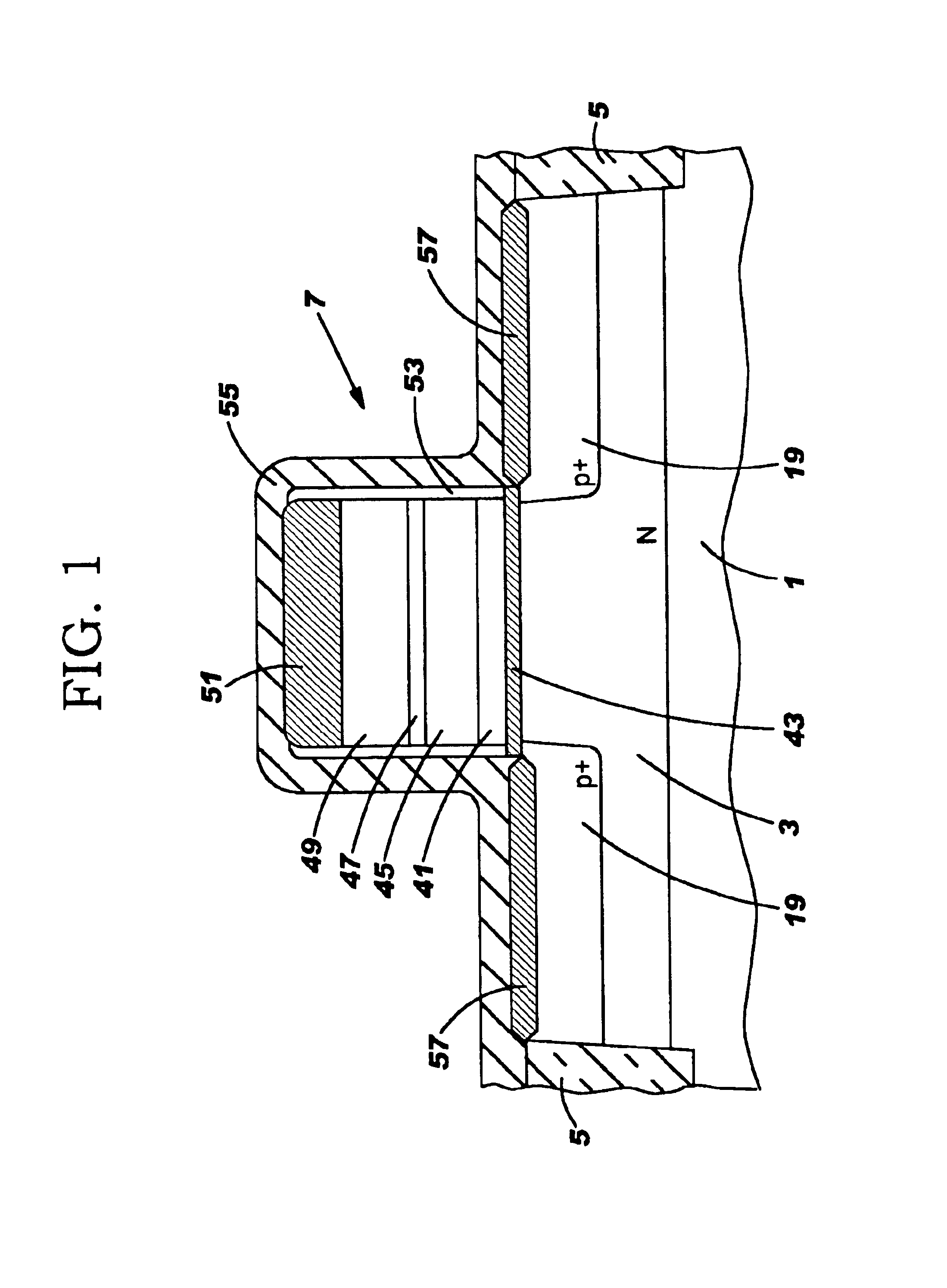
[0022]With reference to FIG. 1, there is shown a cross-section of a pFET with a gate stack structure, as provided in accordance with the present invention. Other than the gate stack structure, the arrangement is a conventional configuration, as is understood by those skilled in the art, and represents only a portion of an integrated circuit structure wherein other pFETs and complementary nFETs may be fabricated on the same substrate. The pFET shown would typically be fabricated on p-type silicon (Si) substrate material (not shown) with p-type expitarial layer 1 formed thereon. A p-type dopant impurity is typically ion implanted into this selected region and an n-type well 3 is formed in the epitaxial layer 1. An nFET on this same substrate would be formed by masking the pFET region with a photoresist, for example, and then ion implanting on an n-type dopant into the nFET region. Shallow trench isolating regions 5 are formed which define the active region. An oxide layer 43 is then f...


PUM

PropertyMeasurementUnit
diameteraaaaaaaaaa
grain sizeaaaaaaaaaa
thicknessaaaaaaaaaa

Abstract

A multi-layered gate electrode stack structure of a field effect transistor device is formed on a silicon nano crystal seed layer on the gate dielectric. The small grain size of the silicon nano crystal layer allows for deposition of a uniform and continuous layer of poly-SiGe with a [Ge] of up to at least 70% using in situ rapid thermal chemical vapor deposition (RTCVD). An in-situ purge of the deposition chamber in a oxygen ambient at rapidly reduced temperatures results in a thin SiO2 or SixGeyOz interfacial layer of 3 to 4A thick. The thin SiO2 or SixGeyOz interfacial layer is sufficiently thin and discontinuous to offer little resistance to gate current flow yet has sufficient [O] to effectively block upward Ge diffusion during heat treatment to thereby allow silicidation of the subsequently deposited layer of cobalt. The gate electrode stack structure is used for both nFETs and pFETs.

Description

BACKGROUND OF THE INVENTION[0001]1. Field of the Invention[0002]The present invention relates to a field effect transistor structures and, more particularly, to a field effect transistor structures with a multi-layered gate electrode structures and process of making same.[0003]2. Background and Related Art[0004]Various types of integrated circuits are fabricated on semiconductor substrates and p-channel type field effect transistors and n-type field effect transistors are major circuit components of the integrated circuits. The desire for increased speed and density, however, has resulted smaller and smaller gate electrodes and extremely thin gate insulating layers. This has, in turn, resulted in what has been called the “short channel” effect which tends to occur in field effect transistors due to narrow gate widths.[0005]One solution to the problem of “short channel” effect has been the introduction of dopant impurity, opposite to the channel conductivity, into the gate electrode....

Claims


Application Information

Patent Timeline
Patent Type & Authority Patents(United States)
IPC IPC(8): H01L21/02H01L29/76H01L29/24H01L29/02H01L21/335H01L29/66H01L31/072H01L31/06H01L31/119H01L31/115H01LH01L21/336H01L21/8238H01L29/49
CPCH01L21/28052H01L21/28061H01L21/2807H01L21/823835H01L21/823842H01L29/4916H01L29/4925H01L29/665
Inventor CHAN, KEVIN K.CHEN, JIAHUANG, SHIH-FENNOWAK, EDWARD J.
Owner GLOBALFOUNDRIES U S INC
Why Eureka
Try Eureka