Luminescent device and process of manufacturing the same

a technology of luminescent devices and manufacturing processes, applied in the field of luminescent devices, can solve the problem of insufficient luminescence and achieve the effect of reducing resistan

Inactive Publication Date: 2005-08-23
SEMICON ENERGY LAB CO LTD
View PDF23 Cites 15 Cited by
  • Summary
  • Abstract
  • Description
  • Claims
  • Application Information

AI Technical Summary

Benefits of technology

[0013]Thus, an object of the present invention is as follows: by using a material which can transmit light in the same way as the transparent conductive film which has been used so far as the anode and further has a lower resistance than the transparent conductive film, the device property of a luminescent device is made higher than in the conventional cases using the transparent conductive film.

Problems solved by technology

By forming the anode having the slits, the area of the anode becomes small to result in a problem that an electric field is not uniformly applied to an organic compound layer and thus sufficient luminescence cannot be obtained.

Method used


Image

  • Luminescent device and process of manufacturing the same
  • Luminescent device and process of manufacturing the same
  • Luminescent device and process of manufacturing the same

Examples


example 1

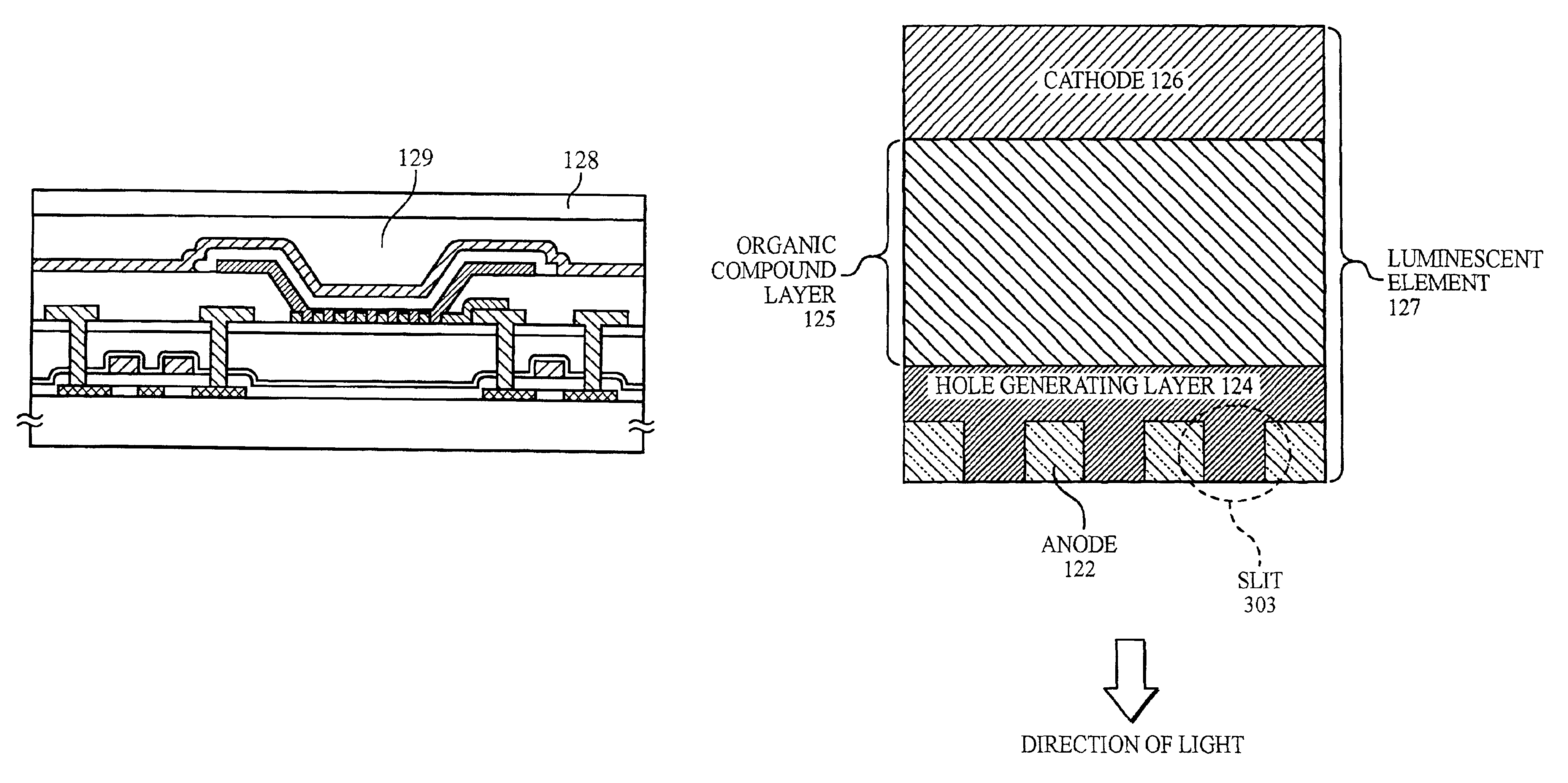
[0062]Referring to FIG. 5, an element structure of a luminescent element which the luminescent device of the present invention has will be described in the present example.

[0063]In FIG. 5, reference number 501 represents an anode having slits 502. The anode 501 can be made of a metal film such as a platinum (Pt), chromium (Cr), tungsten (W) or nickel (Ni) film. In the present example, the thickness of the anode 501 is set to 30 nm.

[0064]Next, a hole generating layer 505 is formed by co-evaporating an electron receptor 503 and a low molecule material 504. In the present example, as the electron receptor, the same material as described in the above-mentioned embodiments can be used. However, as the low molecule material 504, a hole-injecting material is used.

[0065]As the hole-injecting material, a phthalocyanine material can be used, examples of which include copper phthalocyanine (CuPc) and non-metal phthalocyanine (H2PC).

[0066]In the present example, a hole generating layer 505 made...

example 2

[0078]Referring to FIG. 6, a case in which mixture layers are formed in the luminescent element described in Example 1 will be described in the present example.

[0079]In FIG. 6, reference number 601 represents an anode having slits 602, and reference number 605 represents a hole generating layer formed by co-evaporating an electron receptor and a low molecule material.

[0080]A hole injection layer 607, a hole transport layer 608, a luminescent layer 609, and an electron transport layer 610 are successively deposited on the hole generating layer, whereby an organic compound layer 606 can be formed. For the formation thereof, it is advisable to refer to Example 1.

[0081]In the present example, mixture layers are formed between the luminescent layer 609 and the hole transport layer 608 contacting the luminescent layer 609, and between the luminescent layer 609 and the electron transport layer 610 contacting the luminescent layer 609.

[0082]In the present example, the mixture layer formed b...

example 3

[0086]In the present example, a luminescence device wherein luminescent elements which emit red, green and blue light rays are formed will be described. In the present example, the hole generating layer 124 is formed as illustrated in FIG. 1E, and subsequently different materials are used in luminescent layers to form an organic compound layer emitting different color light rays. Since co-evaporation is used as all methods of forming the luminescence layers, the luminescent layers can be made from the materials different for respective pixels, using metal masks when the layers are formed.

[0087]In the present example, a metal mask is used to form luminescent layers emitting red light rays (hereinafter referred to as red color luminescent layers). As the material used to form the red color luminescent layers in the present example, a known material may be used. All of the red color luminescent layers formed in the luminescent device may be formed at the same time, or may be successive...


PUM


Abstract

An object is to improve the element characteristic of a luminescent element. In an anode 122 connected to a drain interconnection 120 of a current-controlling TFT 202, slits are made. A transparent hole generating layer 124 is formed on the anode 122. Since the slits are made, luminescence can be taken out even if a light-shielding metal film is used as the anode 122. Since the hole generating layer 124 has semiconductivity, an electric field applied from the anode 122 to an organic compound layer 125 can be made uniform. Since holes are generated in the hole generating layer 124, the density of carriers injected from the anode 122 can be made high. In this way, a luminescent element having a low driving voltage and a high brightness can be manufactured.

Description

BACKGROUND OF THE INVENTION[0001]1. Field of the Invention[0002]The present invention relates to a luminescent device using a luminescent element having a film comprising an organic compound which can give fluorescence or luminescence by the application of an electric field (hereinafter referred to as an “organic compound layer”), and a process of manufacturing the same.[0003]In the present invention, the luminescent element means an element wherein an organic compound layer is arranged between a pair of electrodes, and the luminescent device means an image display device or a light-emitting device using the luminescent element. The category of the luminescent device includes all of modules wherein a connector such as a flexible printed circuit (FPC), a tape automated bonding (TAB), or a tape carrier package (TCP) is attached to the luminescent element, modules wherein a printed circuit is attached to the tip of the TAB tape or the TCP, and modules wherein an IC (integrated circuit)...

Claims


Application Information

Patent Timeline
Patent Type & Authority Patents(United States)
IPC IPC(8): G09G3/10G09G3/04H01J1/62H01J1/00H01L27/32H01L51/50H01L51/52H05B33/00
CPCH01L51/5088H01L51/5206G09G2300/0814G09G2310/0251H01L27/3211H01L27/3244H01L51/5052H10K59/35H10K59/12H10K50/155H10K50/17H10K50/813
Inventor YAMAZAKI, SHUNPEI
Owner SEMICON ENERGY LAB CO LTD
Why Eureka
Try Eureka