Semiconductor device with reduced terminal input capacitance

Inactive Publication Date: 2005-08-23
RENESAS ELECTRONICS CORP
View PDF8 Cites 2 Cited by
  • Summary
  • Abstract
  • Description
  • Claims
  • Application Information

AI Technical Summary

Benefits of technology

[0018]Therefore, the main advantage of the present invention is that an input capacitance of a terminal to which the test mode detection circuit is connected can be made approximately equal to an input capacitance of another terminal so that a high speed operation becomes possible. Moreover, the restriction of the position for disp

Problems solved by technology

The reason for purposely applying the super VIH level to a terminal to set the device to the test mode is that there is the fear of a user erroneously setting the device to the test mode if a simple command input alone is required to set the test mode.
When the parasitic capacitance of the terminal is great, the transmission of an input signal becomes slow.
In addition, a higher drivability would be required of a device which outputs a signal in order to drive the terminal, which res

Method used


Image

  • Semiconductor device with reduced terminal input capacitance
  • Semiconductor device with reduced terminal input capacitance
  • Semiconductor device with reduced terminal input capacitance

Examples


first embodiment

[0031

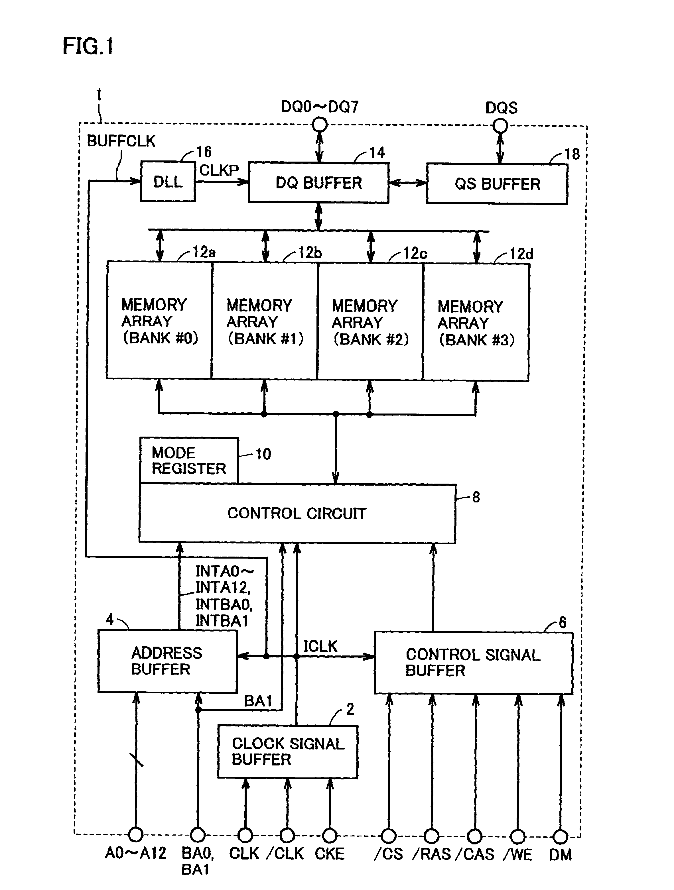
[0032]FIG. 1 is a schematic block diagram showing an arrangement of a semiconductor device 1 of the present invention. Specifically, semiconductor device 1 illustrated in the embodiment is a DDR SDRAM. The present invention, however, can be applied not only to a semiconductor memory device but also to a semiconductor device that needs to be set to a test mode and that requires an input terminal capacitance to be limited to a small amount.

[0033]Referring to FIG. 1, semiconductor device 1 includes an address buffer 4 for receiving external address signals A0 to A12 and bank address signals BA0, BA1 to generate internal address signals INTA0 to INTA12, INTBA0, and INTBA1, a clock signal buffer 2 for receiving external clock signals CLK, / CLK, and a clock enable signal CKE to generate an internal clock signal ICLK, and a control signal buffer 6 for taking in a chip select signal / CS, a row address strobe signal / RAS, a column address strobe signal / CAS, a write enable signal / WE, and a...

second embodiment

[0069

[0070]FIG. 6 is a schematic diagram related to the description of an arrangement for detecting a super VIH level of a semiconductor device according to the second embodiment.

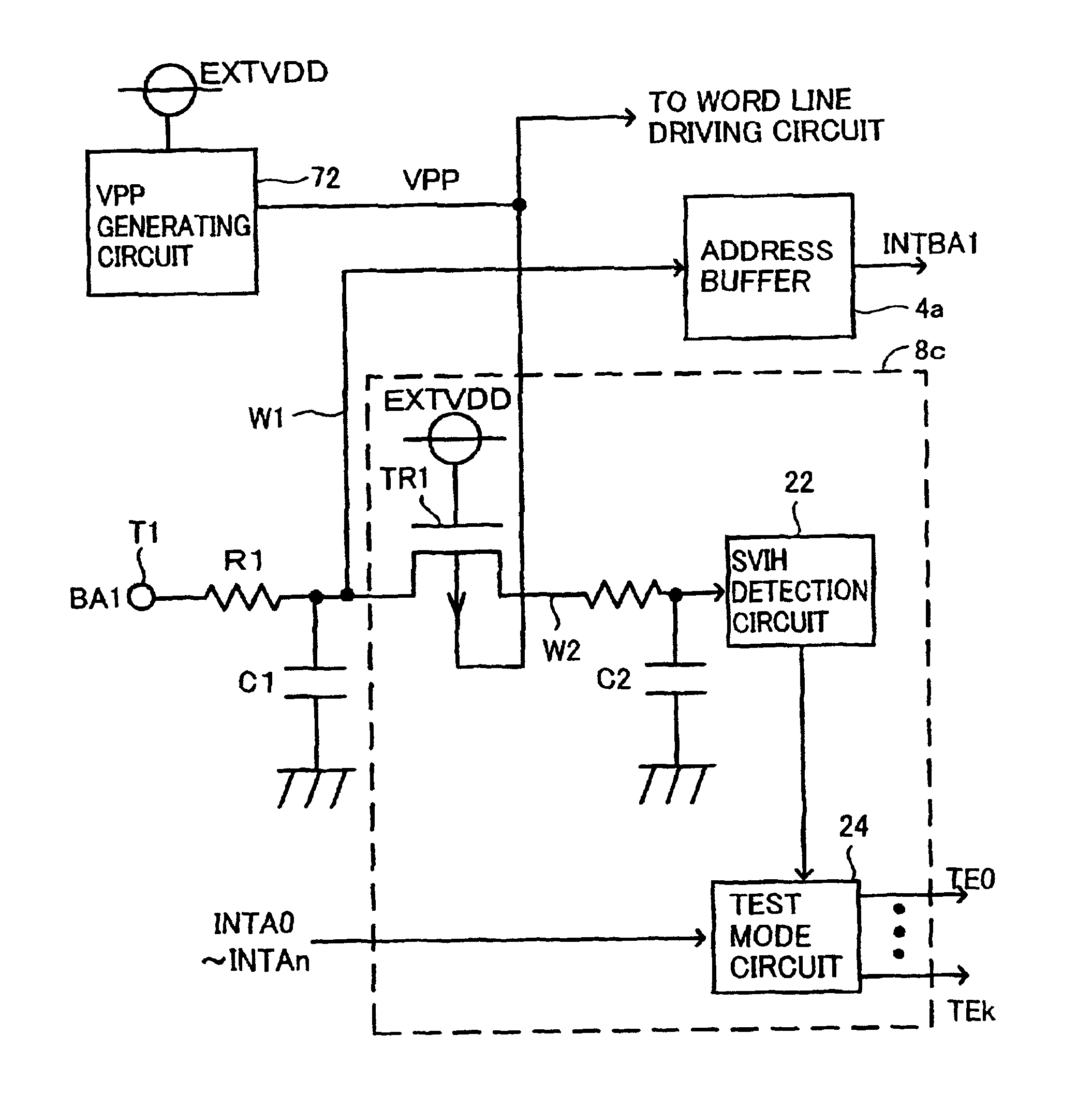
[0071]Referring to FIG. 6, a DRAM, for instance, includes a VPP generating circuit 72 for receiving an external power-supply potential EXTVDD to generate a boosted potential VPP. Boosted potential VPP is used, for instance, as a driving potential of a word line for performing a row selection of a plurality of memory cells arranged in a matrix of rows and columns included in each of memory arrays 12a to 12d of FIG. 1. Boosted potential VPP is supplied from VPP generating circuit 72 to a word line driving circuit.

[0072]The semiconductor device according to the second embodiment includes a control circuit 8b in place of control circuit 8a shown in FIG. 2. Control circuit 8b differs from control circuit 8a in that a gate of a P-channel MOS transistor TR1 receives boosted potential VPP. The arrangement of contro...

third embodiment

[0078

[0079]FIG. 8 is a schematic diagram related to the description of an arrangement for detecting a super VIH level of a semiconductor device according to the third embodiment.

[0080]Referring to FIG. 8, the semiconductor device according to the third embodiment includes a control circuit 8c in place of control circuit 8b shown in FIG. 6. Control circuit 8c differs from control circuit 8b in that a gate of a P-channel MOS transistor TR1 receives a power-supply potential EXTVDD and a backgate is coupled to a boosted potential VPP. The arrangement of control circuit 8c in other portions is the same as that of control circuit 8b described with reference to FIG. 6 so that the description will not be repeated.

[0081]FIG. 9 is a cross sectional view related to the description of P-channel MOS transistor TR1 of FIG. 8.

[0082]Referring to FIG. 9, in the third embodiment, the gate of P-channel MOS transistor TR1 is coupled to power-supply potential EXTVDD. In addition, a well 54 is coupled to...


PUM


Abstract

A P-channel MOS transistor is provided between a terminal and an SVIH detection circuit for performing test mode detection. The P-channel MOS transistor is rendered non-conductive when a potential supplied to the terminal that is used commonly for signal input during the test setting and the normal operation is a power-supply potential EXTVDD or below. The SVIH detection circuit detects that a test mode is to be set when the potential at the terminal becomes higher than a prescribed potential. During the normal operation, the terminal is disconnected from the SVIH detection circuit so that the input capacitance of the terminal can be made to be about the same as that of another input terminal, and a high speed operation becomes possible. Moreover, there is no need to take into account the parasitic capacitance of an interconnection line leading to the SVIH detection circuit.

Description

BACKGROUND OF THE INVENTION[0001]1. Field of the Invention[0002]The present invention relates to a semiconductor device having a test mode and a normal mode as operating modes, and more specifically, to a semiconductor device that employs a higher input level in the test mode than in the normal mode.[0003]2. Description of the Background Art[0004]In some cases, a semiconductor device such as a dynamic random access memory (DRAM) and the like has a super VIH level applied at a terminal in order to set the semiconductor device to a test mode. The super VIH level is a high potential level that is greater than the logic high or H level that is employed when the operating mode is the normal mode. For instance, in the semiconductor device which utilizes a power-supply voltage of 3.3V, the super VIH level would be about 5V. When the super VIH level is applied to a prescribed input terminal, the semiconductor device is set to the test mode.[0005]The reason for purposely applying the super V...

Claims


Application Information

Patent Timeline
IPC IPC(8): G01R31/3185G01R31/28G11C11/401G11C7/00G11C29/00H04L1/22G01R31/317G11C29/14
CPCG01R31/31701G11C29/1201G11C29/46G11C29/00
Inventor ITOU, TAKASHITSUKIKAWA, YASUHIKO
Owner RENESAS ELECTRONICS CORP
Why Eureka
Try Eureka