Fixture used to prepare semiconductor specimens for film adhesion testing

a technology of film adhesion and fixation, which is applied in the direction of individual semiconductor device testing, semiconductor/solid-state device testing/measurement, instruments, etc., can solve the problems of notching steps, and reducing the number of polishing steps

Inactive Publication Date: 2005-08-30
APPLIED MATERIALS INC
View PDF5 Cites 21 Cited by
  • Summary
  • Abstract
  • Description
  • Claims
  • Application Information

AI Technical Summary

Benefits of technology

[0029]The sample preparation method disclosed herein eliminates the time-consuming polishing and notching steps required in the traditional sample preparation method. By eliminating these sample preparation steps, the present method reduces sample preparation time to about 10% of that needed for the traditional sample preparation method. Four-point

Problems solved by technology

Adhesion of the layers of additive material to each other and to the semiconductor substrate is very important, because delamination of any one of the layers can lead to device failure.
While such resistance curve behavior is often observed during interface failure, due to the scale of thin film structures, experimental detection of these effects is difficult and generally precluded.
A significant limitation of many thin film adhesion measurement techniques, such as the peel test, blister test, indentation test, is that during debonding, residual stresses in the thin film relax and modify the measured adhesion energy.
The effects of such relaxation on the measured adhesion values call be large, and although such effects can mathematically be included in an analysis, it is frequently difficult to accurately measure residual film stress of a very thin film present on

Method used


Image

  • Fixture used to prepare semiconductor specimens for film adhesion testing
  • Fixture used to prepare semiconductor specimens for film adhesion testing
  • Fixture used to prepare semiconductor specimens for film adhesion testing

Examples


Embodiment Construction

[0048]As a preface to the detailed description, it should be noted that, as used in this specification and the appended claims, the singular form “a”, “an”, and “the” include plural referents, unless the context clearly dictates otherwise. When the term metal or metallic is used, it is understood that this includes metal alloys. Other terms important to an understanding of the invention are defined in context throughout the application.

[0049]For purposes of illustration, the sample preparation method is described below with reference to FIGS. 5A-5G.

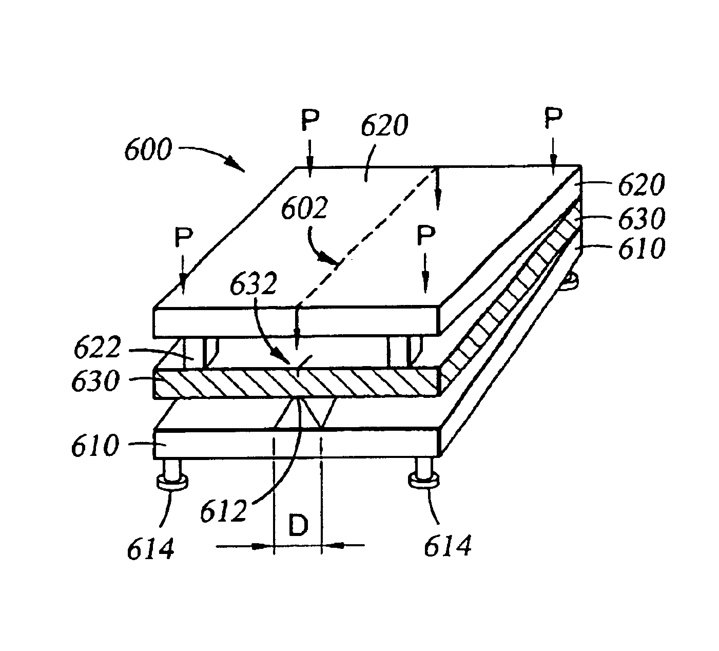
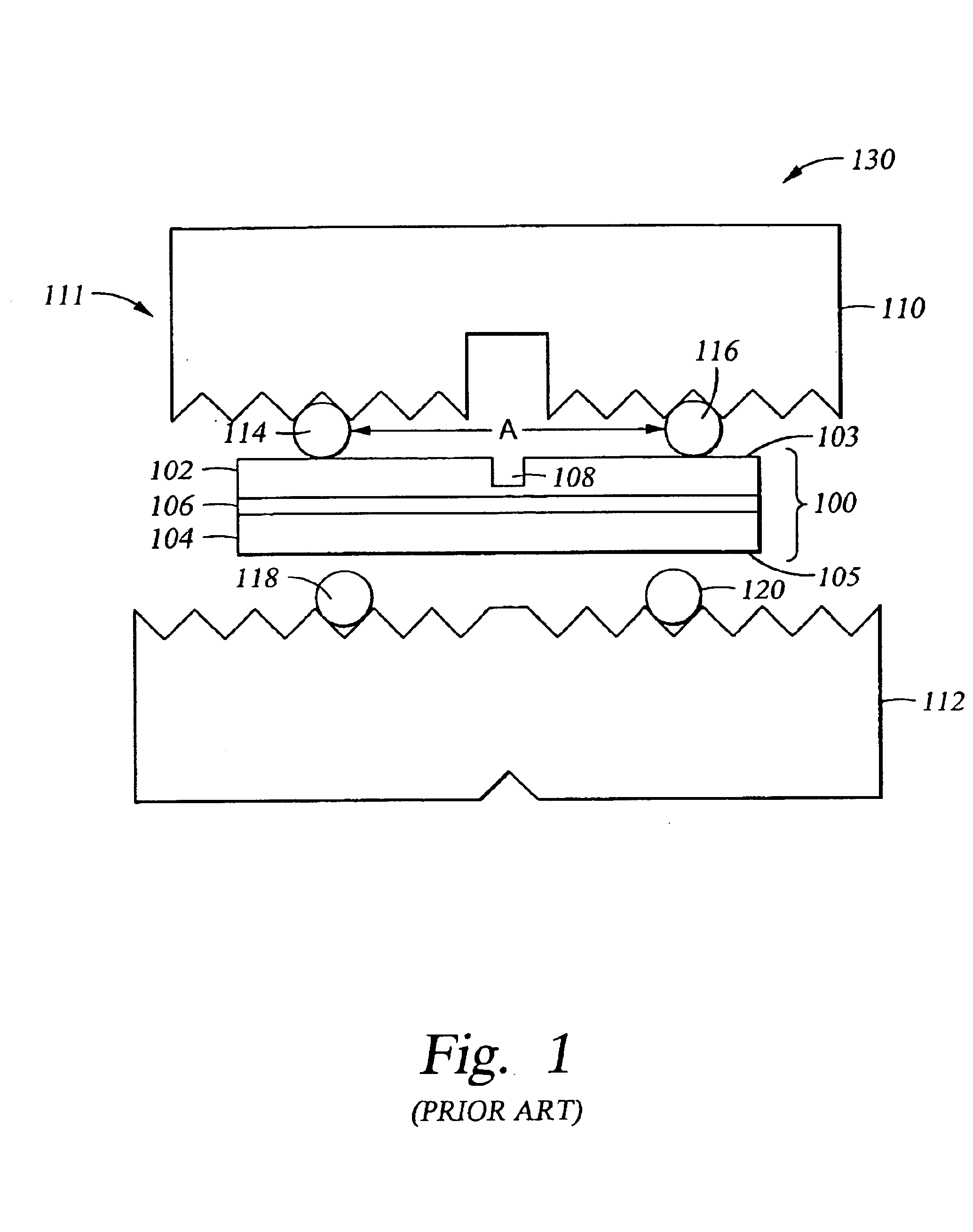
[0050]FIG. 5A shows a cross-sectional side view of a first semiconductor structure 502 and a second semiconductor structure 504 which are used to prepare test specimens for four-point adhesion testing according to the method of the invention. First semiconductor structure 502 consists of a layer 506 of an additive material overlying a crystalline substrate 508. Second semiconductor structure 504 has the same structure as the first semicon...


PUM

PropertyMeasurementUnit
Lengthaaaaaaaaaa
Lengthaaaaaaaaaa
Radiusaaaaaaaaaa

Abstract

The present disclosure pertains to a method of preparing a test specimen for testing of the bonding strength of a layer of additive material to a crystalline substrate, or testing of the bonding strength of one layer of additive material to a second layer of additive material, where both layers of additive material overlie a crystalline substrate. The method includes both test specimen “cutting” from a large sample of material and preparation of an individual test specimen for four-point adhesion testing. Also described is a fixture which is useful for cutting the individual test specimen from the large sample of material.

Description

RELATED APPLICATIONS[0001]This application is a divisional of U.S. Application Ser. No. 10 / 629,071, filed Jul. 28, 2003 now U.S. Pat. No. 6,790,707, which is a continuation-in-part of U.S. application Ser. No. 10 / 435,306, filed May 9, 2003, which is abandoned.FIELD OF THE INVENTION[0002]The present invention pertains to a method of preparing a test specimen for testing of the bonding strength of a layer of additive material to a crystalline substrate, or testing of the bonding strength of one layer of additive material to a second layer of additive material, where both layers of additive material overlie a crystalline substrate.BRIEF DESCRIPTION OF THE BACKGROUND ART[0003]The manufacture of semiconductor devices typically involves the deposition of layers of additive material (i.e., thin films) on a crystalline semiconductor substrate, such as single-crystal silicon or gallium arsenide. Adhesion of the layers of additive material to each other and to the semiconductor substrate is v...

Claims


Application Information

Patent Timeline
IPC IPC(8): H01L23/544
CPCH01L22/34
Inventor CUI, ZHENJIANG
Owner APPLIED MATERIALS INC
Why Eureka
Try Eureka