Flexible compliant interconnect assembly

a technology of interconnects and assemblies, applied in the direction of connection contact member materials, connection devices, printed circuit non-printed electric components associations, etc., can solve the problems of stressing components, soldering these connectors to printed circuit boards, and the use of lead alloy solder and associated chemicals, etc., to achieve a large range of compliance

Inactive Publication Date: 2005-09-06
R&D SOCKETS INC
View PDF111 Cites 74 Cited by
  • Summary
  • Abstract
  • Description
  • Claims
  • Application Information

AI Technical Summary

Benefits of technology

[0012]The present invention is directed to a method and apparatus for achieving a fine pitch interconnect between a flexible circuit member and one or more circuit members with co-planar electrical contacts that have a large range of compliance. The connection with the circuit members can be soldered or solderless. The circuit member can be a printed circuit board, another flexible circuit, a bare-die device, an integrated circuit device, an organic or inorganic substrate, a rigid circuit and virtually any other type of electrical component. The present invention is also directed to an electrical interconnect assembly comprising one or more flexible circuit members electrically coupled to a plurality of circuit members.

Problems solved by technology

The tin lead alloy solder and associated chemicals used throughout the process of soldering these connectors to the printed circuit board have come under increased scrutiny due to their environmental impact.
Additionally, the plastic housings of these connectors undergo a significant amount of thermal activity during the soldering process, which stresses the component and threatens reliability.
The soldered contacts on the connector body are typically the means of supporting the device being interfaced by the connector and are subject to fatigue, stress deformation, solder bridging, and co-planarity errors, potentially causing premature failure or loss of continuity.
In particular, as the mating connector or semiconductor device is inserted and removed from the present connector, the elastic limit on the contacts soldered to the circuit board may be exceeded causing a loss of continuity.
These connectors are typically not reliable for more than a few insertions and removals of devices.
These devices also have a relatively long electrical length that can degrade system performance, especially for high frequency or low power components.
The pitch or separation between adjacent device leads that can be produced using these connectors is also limited due to the risk of shorting.
Such bonding, however, does not lend itself readily to high-density connections because of possible wire breakage and accompanying mechanical difficulties in wire handling.
While this technique has proven successful in providing high-density interconnections for various structures, this technique does not facilitate separation and subsequent reconnection of the circuit members.
The elastomeric material must be compressed to achieve and maintain an electrical connection, requiring a relatively high force per contact to achieve adequate electrical connection, exacerbating non-planarity between mating surfaces.
Location of the conductive elements is generally not controllable.
The interconnection with the circuit elements can be sensitive to dust, debris, oxidation, temperature fluctuations, vibration, and other environmental elements that may adversely affect the connection.
The problems associated with connector design are multiplied when multiple integrated circuit devices are packaged together in functional groups.
One of the major issues regarding these technologies is the difficulty in soldering the components, while ensuring that reject conditions do not exist.
In some circumstances, these joints are generally not very reliable or easy to inspect for defects.
The process to remove and repair a damaged or defective device is costly and many times results in unusable electronic components and damage to other components in the functional group.
Many of the problems encountered with connecting integrated circuit devices to larger circuit assemblies are compounded in multi-chip modules.
Multi-chip modules have had slow acceptance in the industry due to the lack of large scale known good die for integrated circuits that have been tested and burned-in at the silicon level.
As the number of devices increases, the probability of failure increases dramatically.
With the chance of one device failing in some way and effective means of repairing or replacing currently unavailable, yield rates have been low and the manufacturing costs high.

Method used


Image

  • Flexible compliant interconnect assembly
  • Flexible compliant interconnect assembly
  • Flexible compliant interconnect assembly

Examples


Embodiment Construction

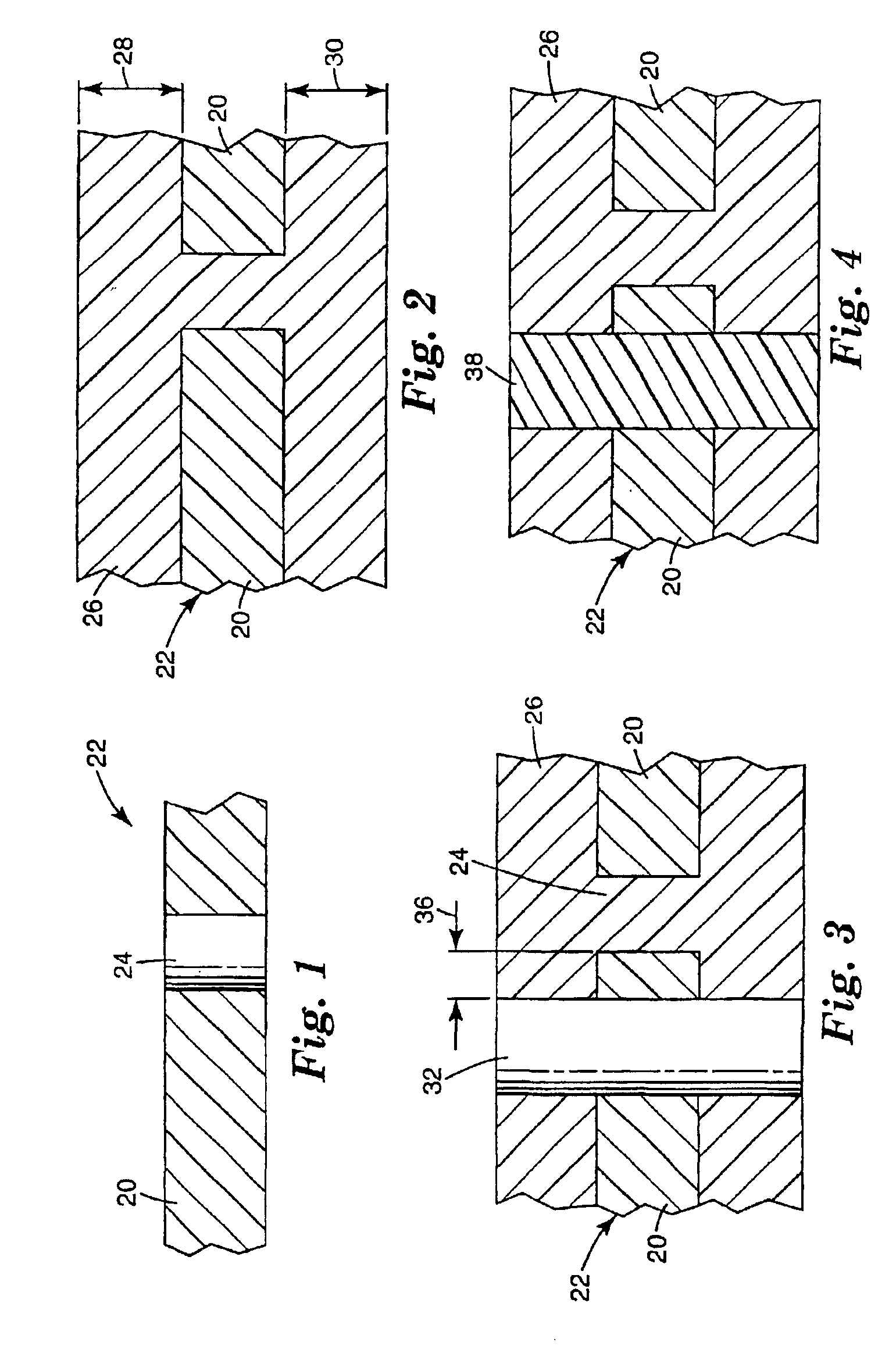
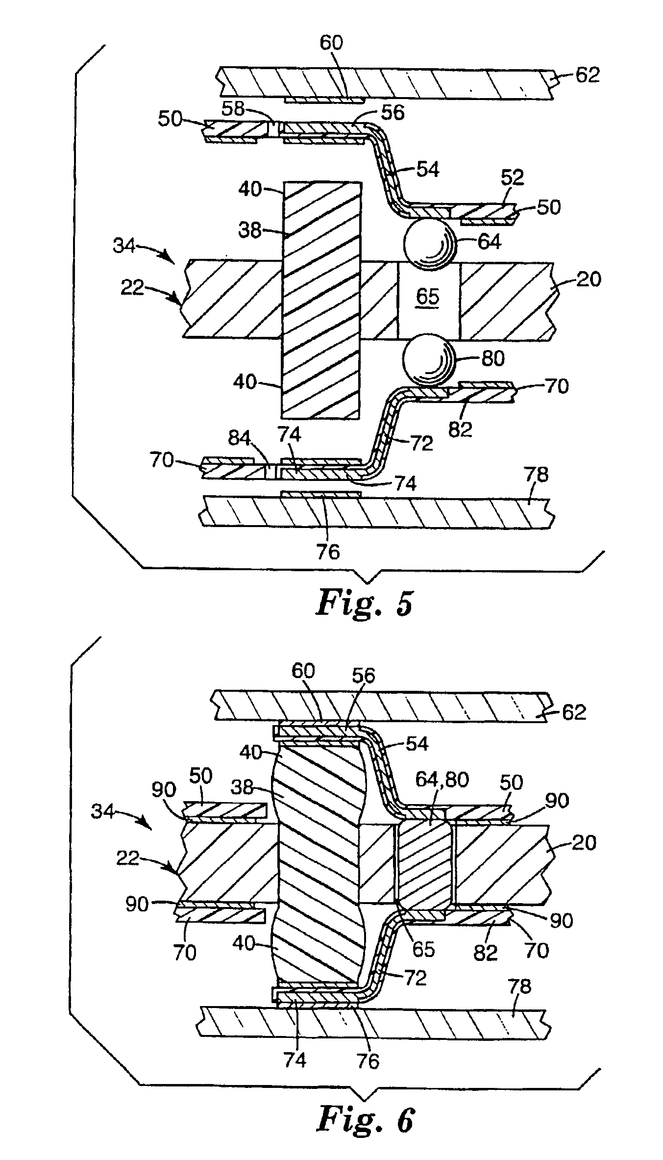
[0048]FIGS. 1-4 illustrate a method of preparing a compliant interconnect 22 in accordance with the present invention (see FIG. 5). The Figures disclosed herein may or may not be drawn to scale. The substrate 20 is perforated to include one or more through holes 24. The holes 24 can be formed by a variety of techniques, such as molding, stamping, laser drilling, or mechanical drilling. The holes 24 can be arranged in a variety of configurations, including one or two-dimensional arrays. As will be discussed below, some embodiments do not require the holes 24. The substrate 20 is typically constructed from a dielectric material, such as plastics, ceramic, or metal with a non-conductive coating. In some of the embodiments discussed below, an electrically active circuit member (see FIG. 11) is substituted for the electrically inactive substrate 20.

[0049]As illustrated in FIG. 2, the substrate 20 is then flooded with one or more masking materials 26, such as a solder mask or other materi...


PUM


Abstract

A method and apparatus for achieving a fine pitch interconnect between a flexible circuit member and another circuit member with co-planar electrical contacts that have a large range of compliance. The interconnect assembly includes a substrate with one or more compliant raised portions. At least one flexible circuit member having a first surface with a plurality of contact pads and a second surface is provided. The substrate is located along the second surface of the flexible circuit member with the compliant raised portions aligned with the contact pads so that the compliant raised portions bias the contact pads with corresponding contact pads on the first circuit member when in a compressive relationship.

Description

[0001]This application claims the benefit of Prov. appl. No. 60 / 177,112 filed on Jan. 20, 2000.FIELD OF THE INVENTION[0002]The present invention is directed to a method and apparatus for achieving a compliant, solderless or soldered interconnect between a flexible circuit member and one or more other circuit members.BACKGROUND OF THE INVENTION[0003]The current trend in connector design for those connectors utilized in the computer field is to provide both high density and high reliability connectors between various circuit devices. High reliability for such connections is essential due to potential system failure caused by misconnection of devices. Further, to assure effective repair, upgrade, testing and / or replacement of various components, such as connectors, cards, chips, boards, and modules, it is highly desirable that such connections be separable and reconnectable in the final product.[0004]Pin-type connectors soldered into plated through holes or vias are among the most comm...

Claims


Application Information

Patent Timeline
Patent Type & Authority Patents(United States)
IPC IPC(8): H01L23/48H01L23/498H01R12/24H01R12/00H05K3/36H05K3/32H05K1/18H01R12/52H01R12/62H05K1/14
CPCH01L23/49811H01L23/49827H01L24/72H01L24/73H01R12/62H05K3/326H05K3/365H01R12/52H01L2224/16H01L2224/48091H01L2224/48227H01L2924/01004H01L2924/01027H01L2924/01029H01L2924/01078H01L2924/01079H01L2924/01082H01L2924/14H01L2924/19041H01L2924/30105H01L2924/3025H01L2924/00014H01L24/48H01L2924/01005H01L2924/01006H01L2924/01033H01L2224/451H01L2924/15787H01L2224/45144H01L2924/12042H01L24/45H01L2224/16227H01L2224/05573H01L2224/05569H01L2224/73257H01L2924/00H01L2924/00015H01L2224/05599H01L2224/05099
Inventor RATHBURN, JAMES J.
Owner R&D SOCKETS INC
Why Eureka
Try Eureka