Component built-in module and method for producing the same

a module and component technology, applied in the direction of printed element electric connection formation, association of printed circuit non-printed electric components, electrical apparatus construction details, etc., can solve the problems of limiting the two-dimensional density of mounting components, increasing the difficulty of releasing heat generated by components, and low thermal conductivity, so as to achieve high-density and small module size, excellent ceramic substrate, and high-performance module

Inactive Publication Date: 2005-09-06
PANASONIC CORP
View PDF33 Cites 56 Cited by
  • Summary
  • Abstract
  • Description
  • Claims
  • Application Information

AI Technical Summary

Benefits of technology

[0010]With the foregoing in mind, it is an object of the present invention to provide a thermal conductive component built-in module in which an inorganic filler can be contained in a thermosetting resin at high density, an active component such as a semiconductor etc. and a passive component such as a chip resistor, a chip capacitor, etc. are buried in the internal portion thereof by a simple method, and a multilayer wiring structure can be formed simply. In the present invention, by selecting an inorganic filler and a thermosetting resin, it is possible to produce a module having a desired performance and to provide a component built-in module that is excellent in a thermal radiation property and a dielectric property.

Problems solved by technology

However, there is a limitation in mounting components two-dimensionally with high density even with the above-mentioned methods.
Furthermore, since these high-density mounted substrates having an inner-via structure are formed of a resin-based material, the thermal conductivity is low.
Therefore, as the mounting density of components becomes higher, it is getting more difficult to release heat that has been generated by the components.
Furthermore, in accordance with high speed and high density, the effect of noise cannot be ignored.
However, in the case where different kinds of materials are fired simultaneously, due to a lag in sintering timing or difference in the shrinkage at the time of sintering, the multilayer substrate may suffer some warping after being fired or an internal wiring may be peeled off.
Therefore, it is possible to include a capacitor, a resistor, or the like, but it is impossible to fire a semiconductor of silicon etc., which lacks in thermal resistant property, simultaneously, and thus the semiconductor cannot be contained.
The ceramic substrate is excellent in the thermal radiation property and capable of containing a capacitor with high dielectric constant, but it is difficult to fire different kinds of materials simultaneously and it is impossible to include a semiconductor.
Also, there is a problem from a viewpoint of cost.
On the other hand, a printed wiring board that can be cured at low temperatures has a possibility of including a semiconductor and is advantageous from the viewpoint of cost, but it is difficult to obtain a high dielectric constant in the case of a composite material mixing a dielectric material, etc. and resin.
In general, the printed wiring board has a low thermal conductivity and inadequate in heat resistance property.
Furthermore, the method of sealing a semiconductor or a capacitor, etc. mounted on the printed wiring board with resin to allow a plurality of layers to be contained has a problem in which individual components can be contained but the thickness of the module itself for the individual components to be buried becomes large, and thus it is difficult to reduce the module volume.
However, the coefficient of thermal expansion of the semiconductor is generally small, and it is extremely difficult to adjust the coefficient of thermal expansion only with a printed wiring board material in the range of operation temperatures.

Method used


Image

  • Component built-in module and method for producing the same
  • Component built-in module and method for producing the same
  • Component built-in module and method for producing the same

Examples


example 1

[0081]In the production of a component built-in module of the present invention, first, a method for producing a sheet material including an inorganic filler and a thermosetting resin will be explained. The sheet material used in this example is prepared by, at first, mixing an inorganic filler and a liquid thermosetting resin with an agitator. The agitator used in this example operates in such a manner that an inorganic filler, a liquid thermosetting resin, and if necessary, a solvent for adjusting the viscosity of the mixture are placed in a predetermined amount in a container, and the container itself is rotated while stirring the mixture in the container. The mixture obtained should be dispersed sufficiently, even if the mixture has a relatively high viscosity. Tables 1 and 2 show the composition mixed in the sheet material for the component built-in module in this example.

[0082]

TABLE 1Composition of thermosetting resinthermosetting resin 1thermosetting resin 2wt.wt.content%Tg(°...

example 2

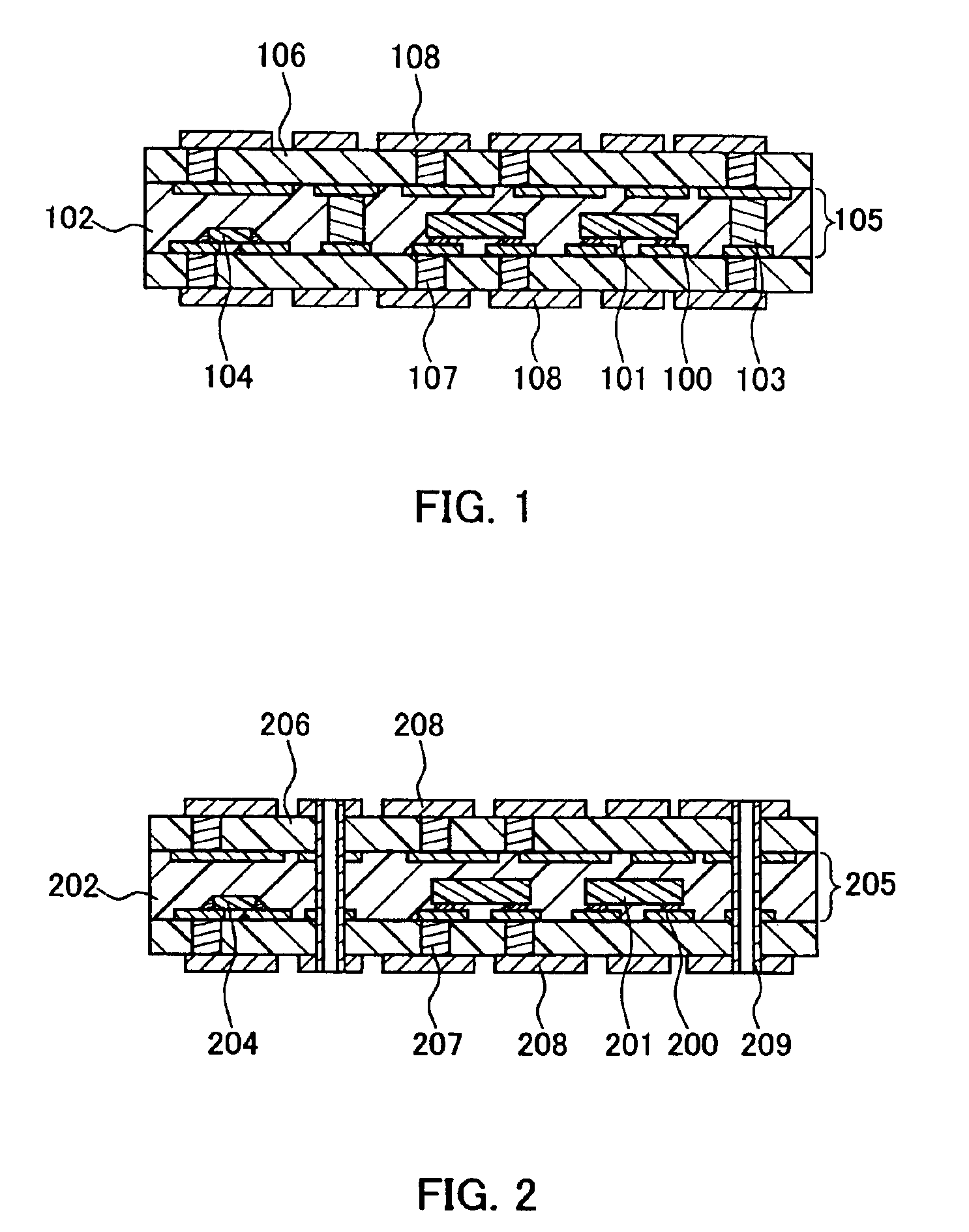
[0093]In Example 2, a module containing a semiconductor was made by using a sheet material same as the case 2 in Example 1.

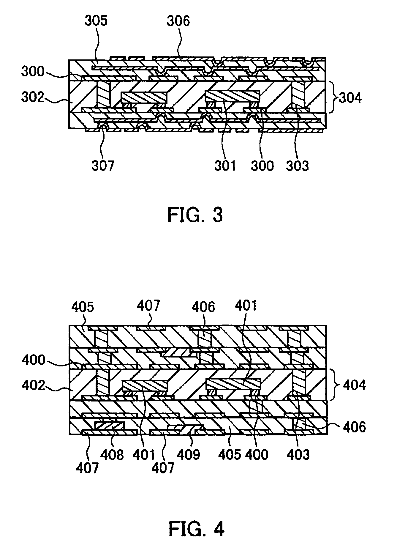
[0094]A 500 μm-thick sheet material 704 in which a through hole was filled with a conductive paste produced under the same conditions as those in Example 1 was prepared (see FIG. 7D). Next, a 70 μm-thick copper foil was formed into a release carrier and further a 9 μm-thick copper was formed on the release carrier by an electrolytic copper-plating method. A wiring pattern was formed by using this release carrier. The release carrier on which the 9 μm-thick copper was formed was chemical-etched by photolithography so as to form a wiring pattern 701 shown in FIG. 7A. A semiconductor and a chip were flip-chip mounted onto the thus produced release carrier with a wiring pattern produced with a solder bump. Furthermore, a film-shaped component was formed on a release carrier having another wiring pattern by a printing method. The film-shaped component 711 is a resist...

example 3

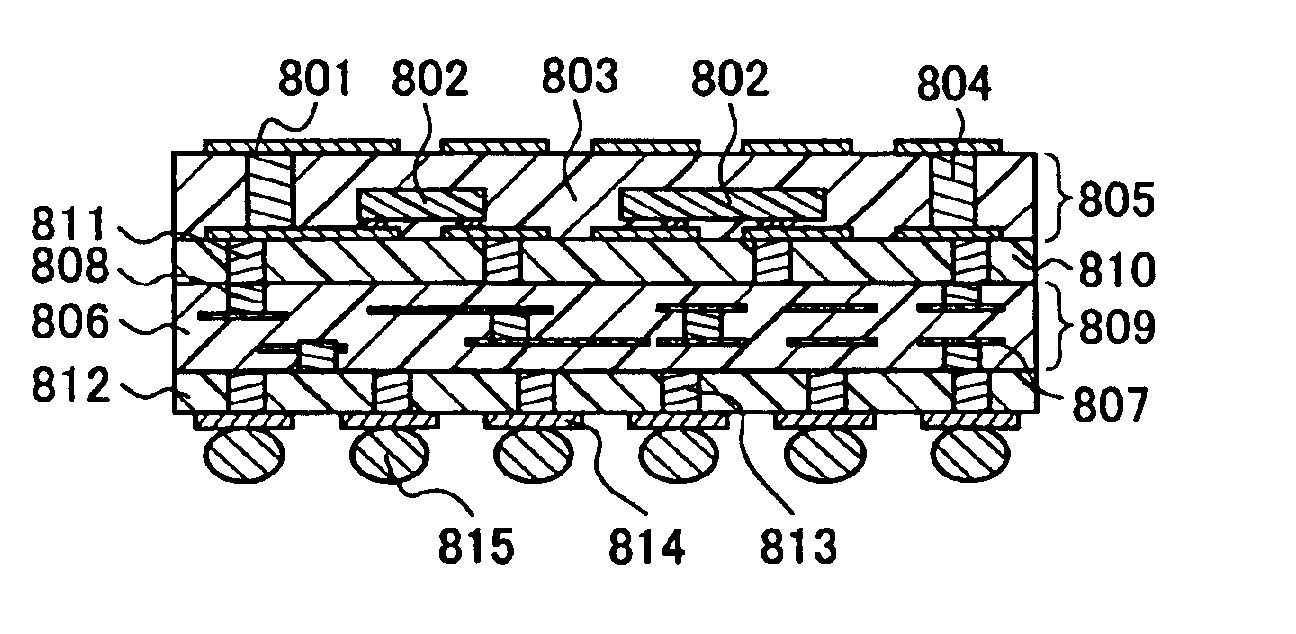
[0098]In Example 3, a higher density module is produced by using a core layer in which a semiconductor is contained in the sheet material as in a case 2 of Example 1 and a multilayer ceramic substrate.

[0099]A core layer 805 containing a semiconductor 802 produced under the same conditions as in Example 1 was used (see FIG. 8A). The thickness of the core layer is 300 μm. Next, the multilayer ceramic substrate 809 and the core layer 805 are laminated with an adhesive layer. Moreover, the ceramic multilayer substrate is produced by using a 20 μm-thick green sheet (“MLS-1000” manufactured by Nippon Electric Glass Co., Ltd.) formed of a low temperature firing material mainly including glass and alumina. Namely, a multilayer ceramic substrate was formed as follows: a through hole having a 0.2 mm diameter was formed on the green sheet by a puncher; the through hole was filled with a conductive paste obtained by mixing silver powders having an average particle diameter of 2 μm as a main com...


PUM

PropertyMeasurementUnit
clock frequencyaaaaaaaaaa
glass transition temperatureaaaaaaaaaa

Abstract

A component built-in module including a core layer formed of an electric insulating material, and an electric insulating layer and a plurality of wiring patterns, which are formed on at least one surface of the core layer. The electric insulating material of the core layer is formed of a mixture including at least an inorganic filler and a thermosetting resin. At least one or more of active components and / or passive components are contained in an internal portion of the core layer. The core layer has a plurality of wiring patterns and a plurality of inner vias formed of a conductive resin. The electric insulating material formed of the mixture including at least an inorganic filler and a thermosetting resin of the core layer has a modulus of elasticity at room temperature in the range from 0.6 GPa to 10 GPa. Thus, it is possible to provide a thermal conductive component built-in module capable of filling the inorganic filler with high density; burying the active component such as a semiconductor etc. and the passive component such as a chip resistor, a chip capacitor, etc. in the internal portion of the substrate; and simply producing a multilayer wiring structure.

Description

[0001]This application is a divisional of application Ser. No. 10 / 033,322, filed Dec. 27, 2001, now U.S. Pat. No. 6,734,542 which application(s) are incorporated herein by reference.BACKGROUND OF THE INVENTION[0002]1. Field of the Invention[0003]The present invention relates to a high-density mounted module containing an active component such as a semiconductor etc. and a passive component such as a resistor, a capacitor, etc.[0004]2. Description of the Prior Art[0005]Recently, with a demand for high performance and miniaturization of electronic equipment, high density and high performance of a semiconductor have been increasingly desired. This leads to a demand for a small size and high-density circuit substrate on which such a semiconductor is to be mounted. In order to meet such demands, a connection method using an inner via that can connect between wiring patterns of LSIs or components in the shortest distance has been developed in various fields in order to achieve higher dens...

Claims


Application Information

Patent Timeline
Patent Type & Authority Patents(United States)
IPC IPC(8): H01L23/538H01L23/48H01L23/52H01L23/498H05K1/18H01L21/48H05K3/20H05K3/40H05K3/46
CPCH01L21/4857H01L23/5384H01L23/5385H01L23/5389H05K1/187H05K1/188H01L23/49816Y10T29/49165H01L2224/16225H01L2924/01046H01L2924/01078H01L2924/01079H01L2924/15311H01L2924/19105H01L2924/3011H05K3/20H05K3/4069H05K3/4602H05K3/4614H05K3/462H05K3/4652H05K2201/0209H05K2201/10378H05K2203/061H01L2924/01019Y10S438/977H01L2224/45144H01L2924/00014H01L2924/3511H01L2924/00H01L2224/0401
Inventor NAKATANI, SEIICHISUGAYA, YASUHIROASAHI, TOSHIYUKIKOMATSU, SHINGO
Owner PANASONIC CORP
Why Eureka
Try Eureka