Low leakage heterojunction vertical transistors and high performance devices thereof

a vertical transistor and heterojunction technology, applied in the field of metal insulator semiconductor field effect transistors, can solve the problem of relativly easy to do so with vertical devices or finfets, and achieve the effects of avoiding tradeoffs in conventional si technology, superb performance and scalability, and optimizing drive current and leakage curren

Inactive Publication Date: 2005-09-13
GLOBALFOUNDRIES INC
View PDF1 Cites 441 Cited by
  • Summary
  • Abstract
  • Description
  • Claims
  • Application Information

AI Technical Summary

Benefits of technology

[0012]The objective of this invention is to provide a device structure that has superb performance and scalability. By using 2-dimensional bandgap engineering, the tradeoffs in the conventional Si technology can be avoided, and the drive current and leakage current ...

Problems solved by technology

While it is not practical to integrate a nMOSFET on a (100) plane and a pMOSFET on a (110) plane usi...

Method used


Image

  • Low leakage heterojunction vertical transistors and high performance devices thereof
  • Low leakage heterojunction vertical transistors and high performance devices thereof
  • Low leakage heterojunction vertical transistors and high performance devices thereof

Examples


first embodiment

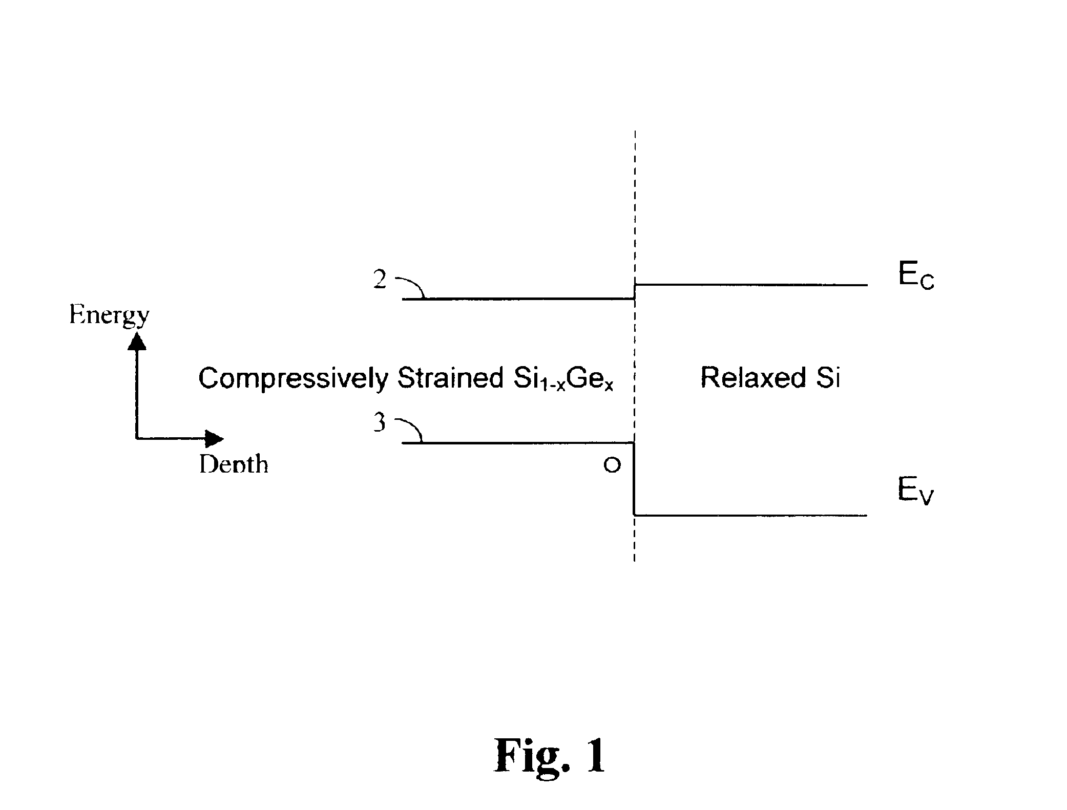
[0030]FIG. 4 shows the top view of a vertical device 160 (not to scale). FIG. 5 shows the cross sectional view of the first embodiment which is a compressively strained SiGeC vertical pMOSFET 160 comprising a vertical column 5000 comprising several layers or regions, such as a source layer or region 164, a body layer or region 163, and a drain layer or region 162, with a channel layer or region 165, an insulator layer or region 166, and a gate electrode layer or region 167 on the sidewalls. Vertical column or mesa 6000 forms vertical device 160. When SiGe layer or region 164 is highly strained, its critical thickness is rather small. The more strain in the layer, the thinner is the critical thickness at which the stained layer starts to relax. The critical thickness is understood in the art as a thickness where defects are generated within a layer or region to relieve its strain so that the layer or region relaxes towards its natural lattice spacing. The lattice spacing is determine...

second embodiment

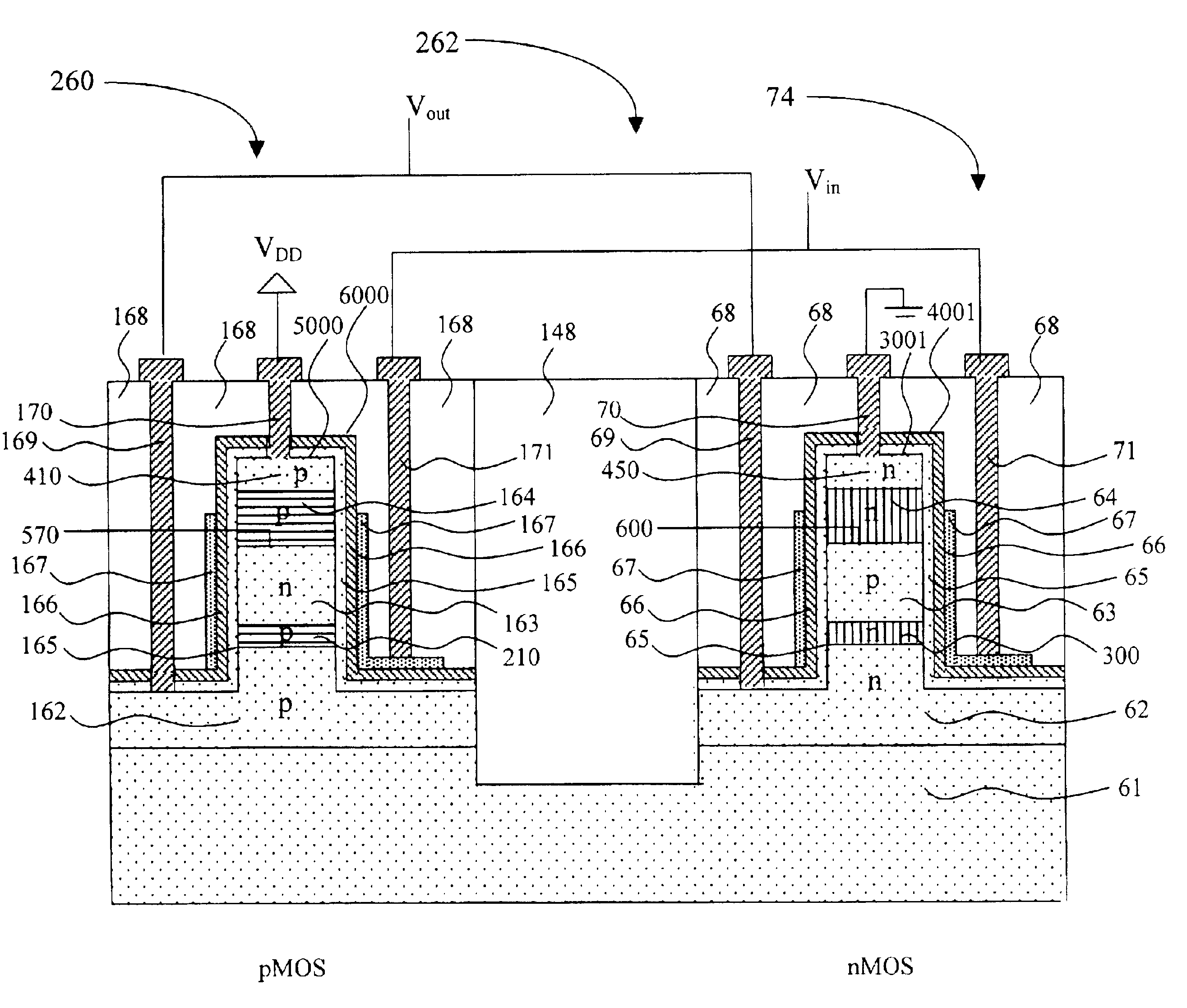
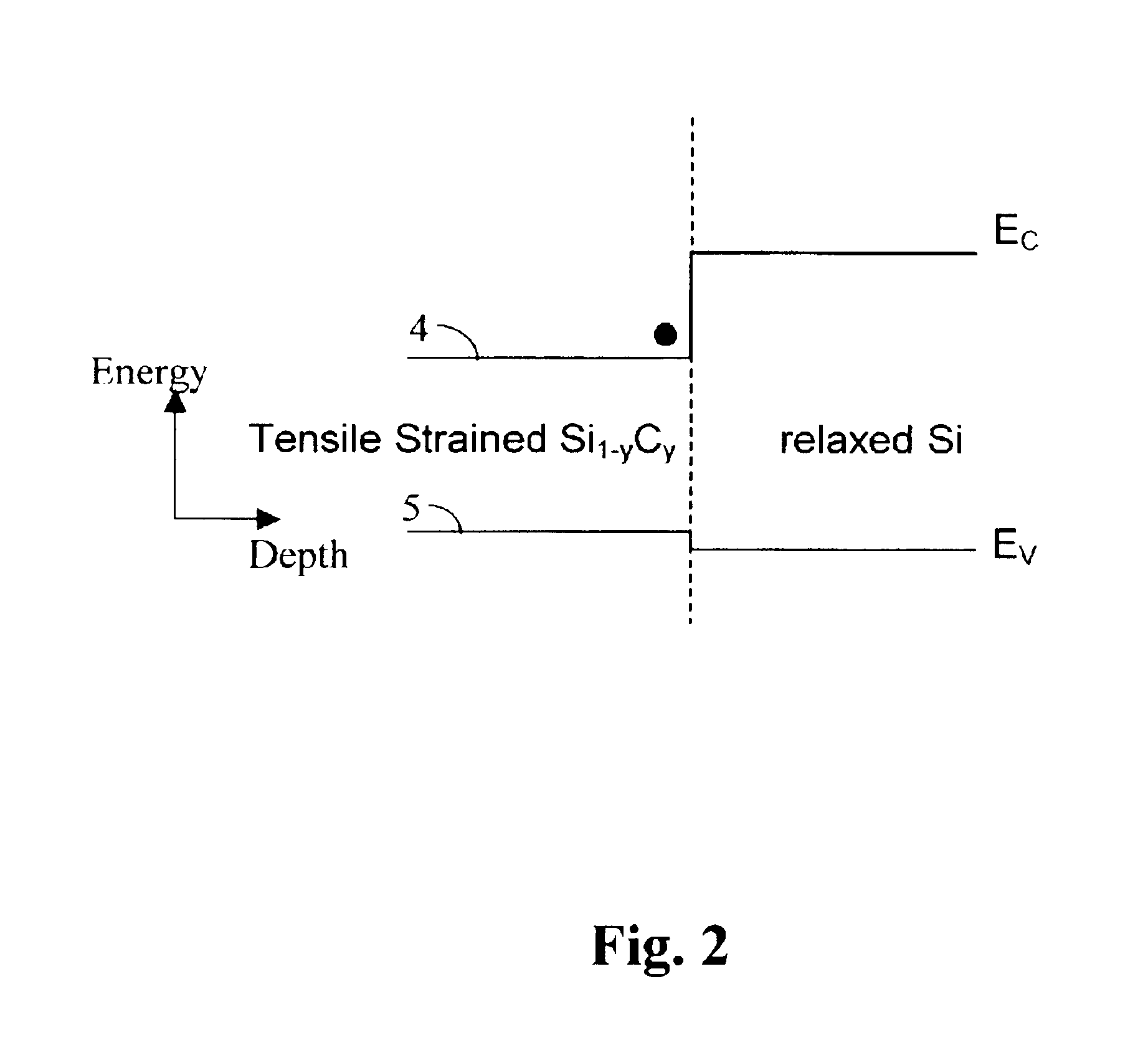
[0083]FIG. 10 shows the vertical CMOS 362, similar to FIG. 9 except for the nMOSFET 374. The nMOSFET 374 has a tensile-strained silicon channel 65 built on a relaxed SiGe body 63. Body 63 is relaxed with respect to virtual substrate 62. The advantage of having tensile-strained silicon as the channel is the higher electron mobility. The mesa 3001 orientation is shown in FIG. 8B, where the p-channel is in the plane (110) and the n-channel is in the plane (100) for higher hole and electron mobilities.

[0084]A method of preparing an inverter made of the vertical field effect CMOS transistors is described comprising the steps of:[0085]forming a relaxed Sil-iGei epitaxial layer or region 62 on a first single crystalline substrate 61, doping the Sil-iGei epitaxial layer or region 62 n-type to a concentration level greater than 1×10¹⁹ atoms / cm3,[0086]forming a carbon-doped SiGe epitaxial layer or region 300 over the n-type Sil-iGei layer or region 62, doping the silicon epitaxial layer or re...


PUM


Abstract

A method for forming and the structure of a vertical channel of a field effect transistor, a field effect transistor and CMOS circuitry are described incorporating a drain, body and source region on a sidewall of a vertical single crystal semiconductor structure wherein a hetero-junction is formed between the source and body of the transistor, wherein the source region and channel are independently lattice strained with respect the body region and wherein the drain region contains a carbon doped region to prevent the diffusion of dopants (i.e., B and P) into the body. The invention reduces the problem of short channel effects such as drain induced barrier lowering and the leakage current from the source to drain regions via the hetero-junction and while independently permitting lattice strain in the channel region for increased mobility via choice of the semiconductor materials. The problem of scalability of the gate length below 100 nm is overcome by the heterojunction between the source and body regions.

Description

CROSS REFERENCE TO RELATED APPLICATIONS[0001]This application is further cross referenced to U.S. patent application Ser. No. 10 / 463,038 by Q. Ouyang and Jack O. Chu, the inventors herein, filed herewith, entitled “Ultra Scalable High Speed Heterojunction Vertical N-channel MISFETs and Methods Thereof” which is directed to vertical N-channel MISFETs which is incorporated herein by reference and assigned to the assignee herein.[0002]This application is further cross referenced to U.S. patent application Ser. No. 10 / 462,933 by Q. Ouyang and Jack O. Chu, the inventors herein, filed herewith, entitled “High Speed Lateral Heterojunction MISFETs Realized by 2-dimensional Bandgap Engineering and Methods Thereof” which is directed to lateral Heterojunction MISFETs which is incorporated herein by reference and assigned to the assignee herein.FIELD OF THE INVENTION[0003]This invention relates to semiconductor transistors and, more particularly, to a metal insulator semiconductor field effect ...

Claims


Application Information

Patent Timeline
IPC IPC(8): H01L21/70H01L21/8238H01L27/092H01L21/336H01L29/12H01L29/78H01L29/786
CPCH01L21/823807H01L21/823885H01L29/778H01L29/7781H01L29/7782H01L29/7789H01L29/045H01L29/161H01L29/165H01L29/7828
Inventor OUYANG, QIQING CHRISTINECHU, JACK OON
Owner GLOBALFOUNDRIES INC
Why Eureka
Try Eureka