Sequential build circuit board

a new type of circuit board and build technology, applied in the direction of photomechanical equipment, printed element electric connection formation, instruments, etc., can solve the problems of increasing complexity of mlbs, shrinking of resinous portion of the laminate, and inability to economically form the dimensions desired by the industry by the time of manufacturing, etc., to achieve significant increase in the rigidity of the board, increase the flexural strength or rigidity of the mlb

Inactive Publication Date: 2005-09-20
SHIPLEY CO LLC
View PDF8 Cites 43 Cited by
  • Summary
  • Abstract
  • Description
  • Claims
  • Application Information

AI Technical Summary

Benefits of technology

[0024]In the above process, glass fiber reinforced copper clad epoxy substrates, required to provide flexural strength or rigidity to a conventional board, are not required for boards fabricated in accordance with process disclosed herein. In accordance with an additional embodiment of the invention, the flexural strength or rigidity of the MLB may be increased by incorporation of metal deposited reinforcing members passing vertically through all or a portion of the thickness of the board, horizontally over the surface of one or more layers of the board, by the use of an applied reinforcing member as the final layer in the construction of the board, or any combination of these approaches. When using deposited metal as the reinforcing material, the reinforcing members are desirably formed by metal deposition simultaneously with the deposition of metal during the process for formation of interconnections or vias and circuit lines. When using vertical reinforcing members, they are built to the full thickness of the board as each sequential layer of the MLB is formed. This is accomplished by forming one or more recesses in successive imaged dielectric coatings where the recesses are in registration with each other. The recesses are formed at the time the coating is imaged for interconnections or circuit lines. The recesses for interconnections or circuit lines and the reinforcing members are then selectively metal plated during the metal plating sequence. The sequential build-up of metal in the recesses defining the reinforcing member results in the reinforcing members passing through a portion of or the full thickness of the board. In this embodiment of the invention, the reinforcing members may be in the form of pegs, rectangular bars located at the edges or within the board, or any other shape consistent with acceptable circuit design. By strategic location of an array of reinforcing members within the board, board rigidity may be significantly increased.

Problems solved by technology

MLBs have become increasingly complex.
Known commercial procedures now used are incapable of economically forming the dimensions desired by the industry.
However, since lamination is at a temperature above 150° C., the resinous portion of the laminate shrinks during cooling to the extent permitted by the rigid copper cladding.
This problem is exacerbated as feature size decreases.
Consequently, further shrinkage may occur.
The shrinkage may have an adverse affect on dimensional stability and registration between board layers.
Otherwise, the layers will not be aligned and electrical contact between layers will not be achieved.
In addition, during lay-up, air is often trapped in spaces adjacent to signal lines because a solid pre-preg is laid over the signal lines that does not completely fill all recesses between signal lines.
Residual air pockets can cause defects and subsequent problems during use of the multilayer board.
The use of glass reinforced inner and outerlayer materials creates additional problems.
If the glass is not removed, a loss of continuity might occur in the metal deposit.
The attachment of chips and other electrical components to a finished MLB adds additional, costly processing steps to the overall fabrication of an electronic device.
The elevated temperatures cause differential expansion of layers within the board resulting in undesirable pressures within the MLB.

Method used


Image

  • Sequential build circuit board
  • Sequential build circuit board
  • Sequential build circuit board

Examples


Embodiment Construction

General

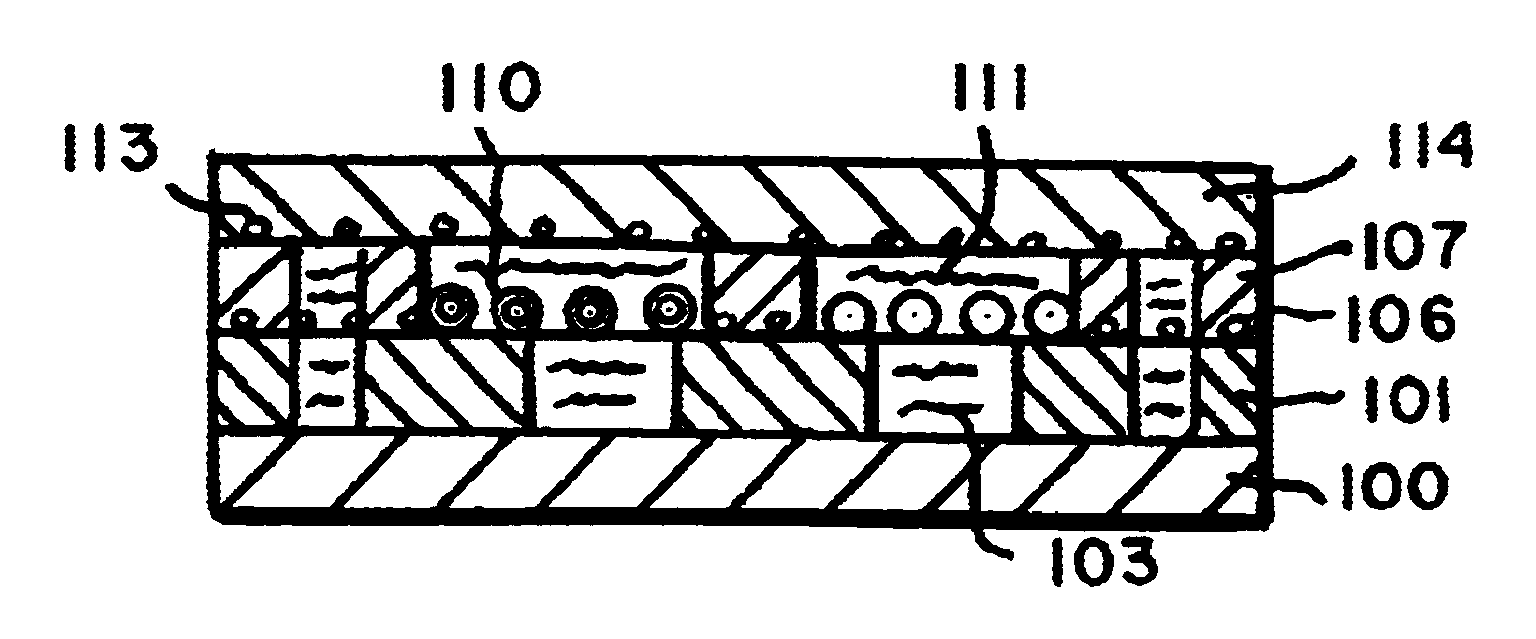
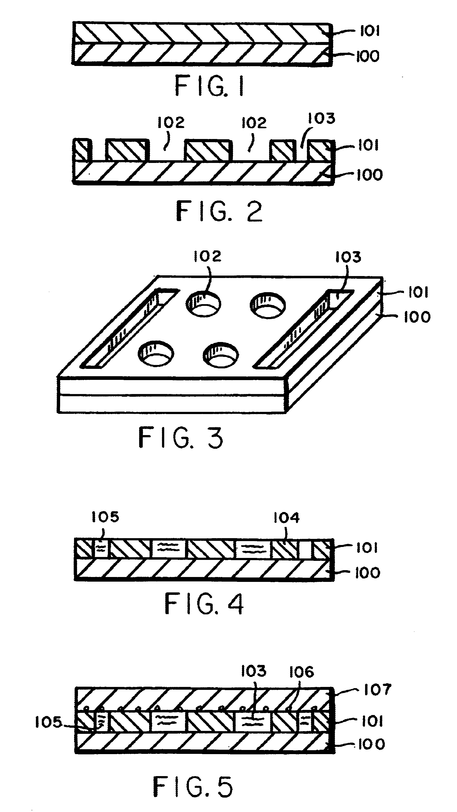
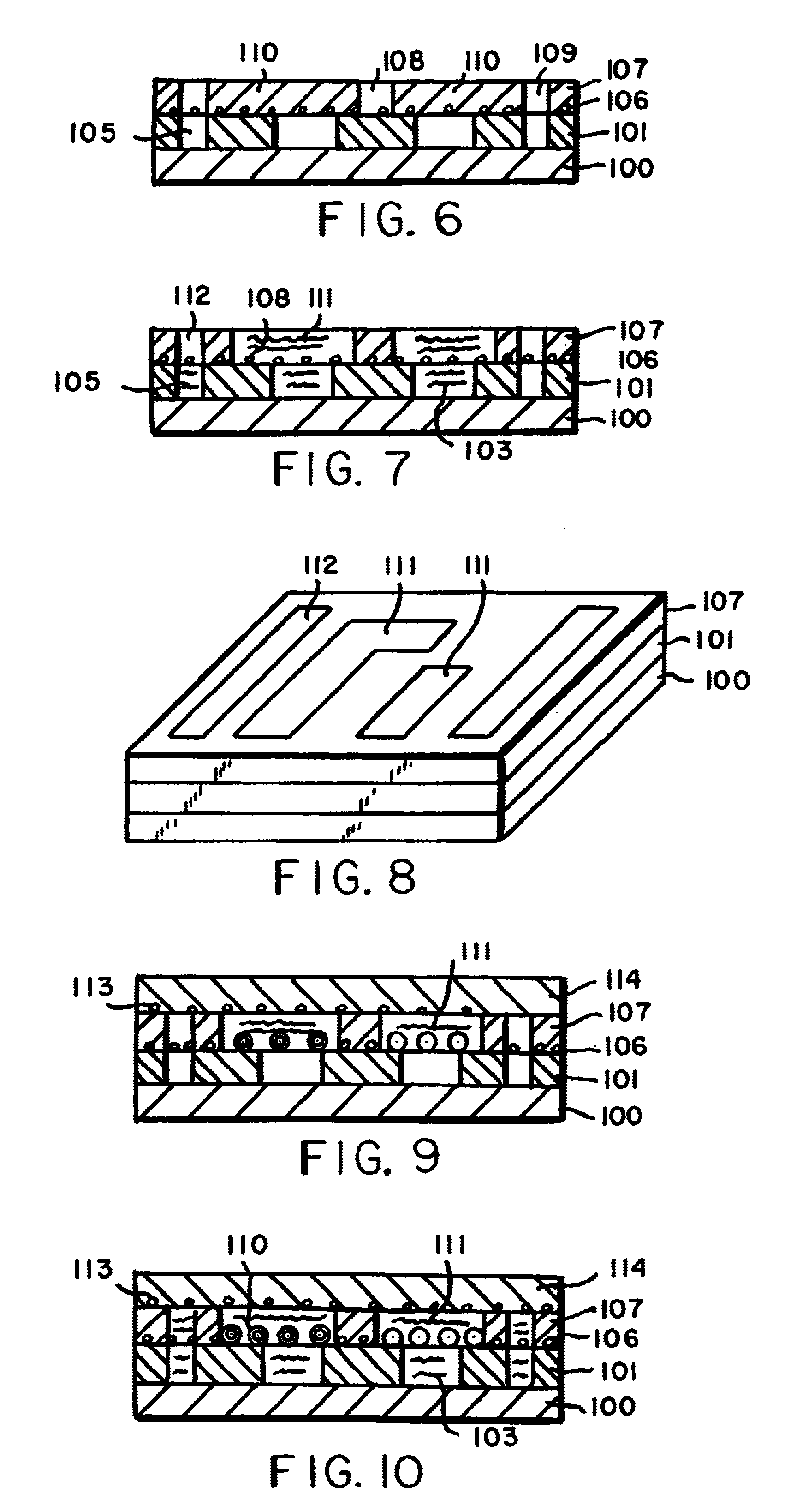
[0031]In the description that follows, the fabrication of an MLB in accordance with the process of the invention will be described first. Materials suitable for use in the process steps will be discussed following the description of the process. In the described processes, unless otherwise stated and for purposes of illustration, the supporting structure for sequential build of the MLB is an electrically conductive temporary platen though it should be understood that other substrates may be used including those that might become a permanent part of the MLB. Examples of such permanent substrates include, for example, a housing for an item of electronic equipment, a ground or power plane, etc. Dielectric coatings used in the process may be Imaged by laser ablation or by exposure and development. Imaging details will be given in the description below for the first disclosed imaging sequence and in the discussion of imaging materials. Thereafter, for brevity, imaging details will...


PUM

PropertyMeasurementUnit
diameteraaaaaaaaaa
diameteraaaaaaaaaa
diameteraaaaaaaaaa

Abstract

A method for manufacture of a circuit board and the board formed by the novel method. The method comprises selective plating of metallic reinforcing members, solder mount pads, signal and interconnections sequentially. The resultant board is desirably free of glass fiber reinforcement.

Description

BACKGROUND OF THE INVENTION[0001]1. Introduction[0002]This invention relates to new multilayered circuit boards and to processes for manufacture of the same. More particularly, the invention relates to new multilayered circuit boards having capacity for increased chip and other component attachment and further characterized by increased circuit density. The multilayered circuit boards are formed by new sequential build procedures.[0003]2. Description of the Prior Art[0004]Multilayer circuit boards (MLBs) permit formation of multiple circuits in a minimum volume or space. They typically comprise a stack of layers where layers of signal lines (conductors) are separated from each other by a layer of dielectric material. The signal lines are in electrical contact with each other by plated holes passing through the dielectric layers. The plated holes are often referred to as “vias”. Such stacks also typically contain power and ground planes.[0005]Known processes for fabricating MLBs are ...

Claims


Application Information

Patent Timeline
Patent Type & Authority Patents(United States)
IPC IPC(8): H01K3/00H01K3/10H05K1/02H05K3/20H05K3/34H05K3/42H05K3/46
CPCH05K3/465H05K1/0271H05K3/205H05K3/3473H05K3/423Y10T29/49117H05K2201/2009H05K2203/0733Y10T29/49165Y10T29/49126Y10T29/49155H05K2201/09781
Inventor SHIPLEY, CHARLES R.GOLDBERG, ROBERT L.SHELNUT, JAMES G.
Owner SHIPLEY CO LLC
Why Eureka
Try Eureka