Supercharge Your Innovation With Domain-Expert AI Agents!

Methods of making and using a floating interposer

a floating interposer and interposer technology, applied in the direction of coupling device connection, final product manufacturing, sustainable manufacturing/processing, etc., can solve the problems of chip cracking, delamination and device breakdown, and high interconnection stress

Inactive Publication Date: 2005-09-20
GLOBALFOUNDRIES INC
View PDF18 Cites 4 Cited by
  • Summary
  • Abstract
  • Description
  • Claims
  • Application Information

AI Technical Summary

Benefits of technology

[0008]In accordance with the teachings of the present invention, internal stresses in chip dies and their electrical interconnection caused by encapsulation and bonding of chip dies to laminate chip carriers are overcome through the use of a floating interposer having an array of connectors extending therethrough and positioned between chip die contacts and circuit card contacts. The floating interposer acts as chip carrier and provides stress relief to the electrical interconnections between chip die and circuit card by moving on its opposing surfaces relative to the CTE rate of the material with which it is in contact.
[0009]The floating interposer of the present invention comprises a flexible and compliant layer of low modulus material having an array of vias plated with copper which vias terminate in copper pads at each end on opposing surfaces of the flexible layer. In addition, the flexible layer may have an array of relatively large holes arranged between the array of vias to produce a “swiss-cheese-like” structure to give more resilience.
[0013]It is a further object of the present invention to provide improved electronic interconnection between chip die device and chip carrier.
[0014]It is yet a further object of the present invention to provide an improved electronic interconnection between chip die and chip carrier such as to reduce internal stress in both the chip die and the electrical interconnections between chip die and chip carrier.
[0015]It is still yet a further object of the present invention to provide a flexible interposer arrangement between chip die and chip carrier which allows the chip die to be connected to the chip carrier without encapsulation of the interconnection points.
[0017]It is yet another object of the present invention to provide a compact, reworkable die solution.

Problems solved by technology

One of the problems encountered with some semiconductor chip die connections to the next level of packaging is the high stress on the interconnections caused by coefficient of thermal expansion (CTE) mismatch.
The CTE thermal mismatch is particularly large where the chip die is connected to laminate chip carriers made of material similar to an epoxy circuit board material.
As circuit densities in chip dies increase, so does the heat generated by these dies thereby compounding the problem with larger temperature variations in its thermal cycle.
This bonding of chip die to chip carrier reduces solder joint stress during thermal cycling but causes the chip die itself to be put under cyclical high internal stress eventually leading to chip cracking, delamination and device breakdown.
As a result of the large thermal mismatch between the die and laminate chip carrier, the cyclical bending over time causes device failure.
Thus, although the use of encapsulation is to prevent the C-4 connections from detaching from fatigue and fracturing over thermal cycling, the bonding action of the encapsulation in itself acts to cause the chips to fracture and separate from the chip carrier.
However, these various efforts typically rely on single or multiple layers of material which are either costly to fabricate or difficult to assemble, and are not totally effective in their purpose.

Method used


Image

  • Methods of making and using a floating interposer
  • Methods of making and using a floating interposer

Examples


Embodiment Construction

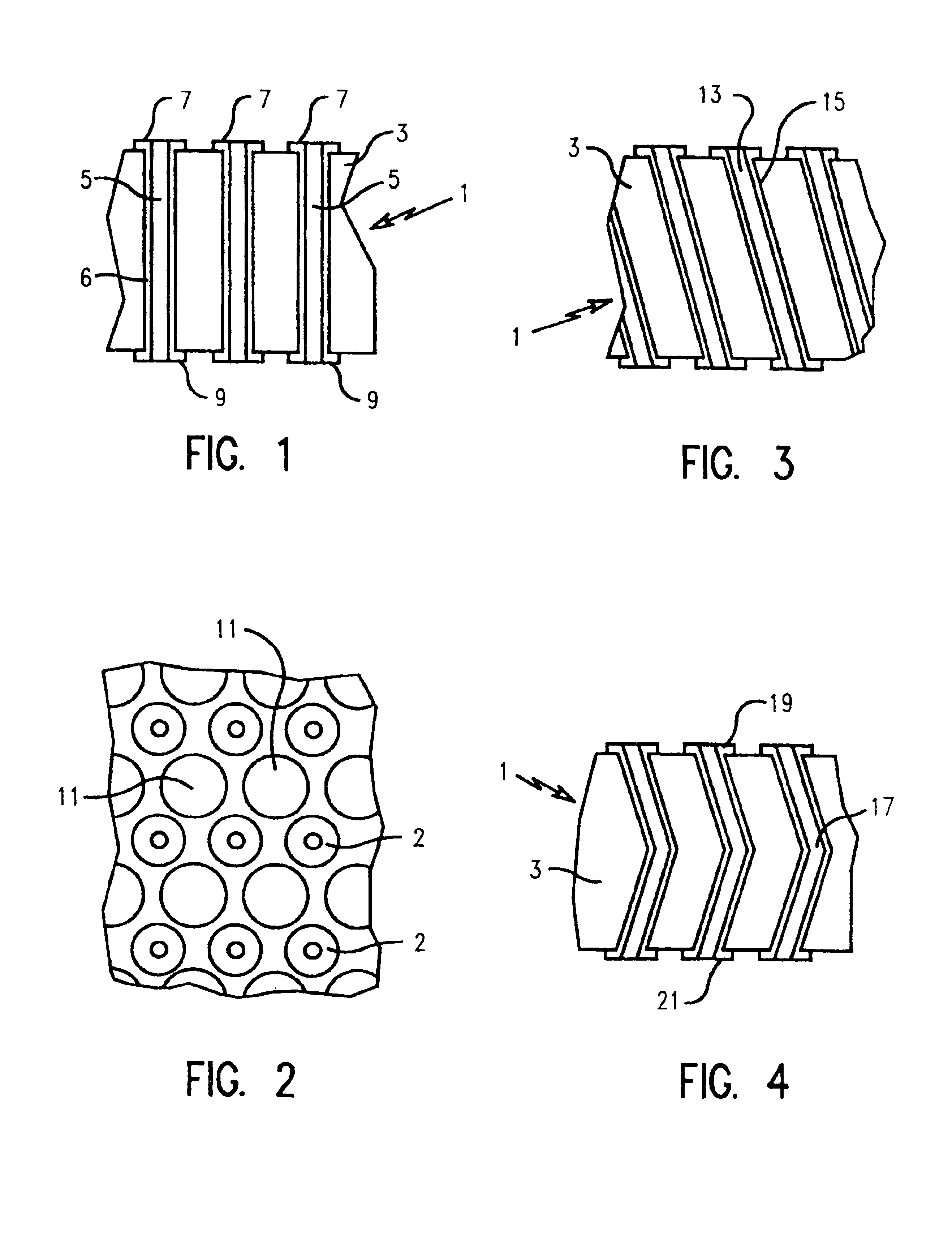
[0029]With reference to FIG. 1, there is shown an interposer arrangement, in partial cross-section, fabricated in accordance with the present invention. Interposer 1 is fabricated from a flexible dielectric layer 3 of low modulus material such as, for example, Rogers 2800 material, Dow 1-4173 material or GE 3281 material. Layer 3 may have an elastic modulus in the range of about 50,000 psi to about 400,000 psi. The thickness of flexible dielectric layer 3 may range between 10 to 15 mils. This may be obtained by laminating several layers of Rogers 2800 material, for example, with heat and pressure to form this thickness. An array of vias 5 are formed in the layer, each approximately 2 mils in diameter. These vias may be fabricated by laser ablation, for example. The array of vias are patterned to match the pattern of connection points on the flip chip die and corresponding connection points on the circuit card chip carrier to which it will be interposed and connected. The vias are th...


PUM

PropertyMeasurementUnit
Temperatureaaaaaaaaaa
Lengthaaaaaaaaaa

Abstract

A flexible, compliant layer of a single low modulus material for connecting a chip die directly to a circuit card without encapsulation. The flexible compliant layer provides stress relief caused by CTE thermal mismatch in chip die and circuit card. An array of copper plated vias are formed in said compliant layer with each via terminating on opposing surfaces of the layer in copper pads. Rather than copper, other metals, such as gold or nickel, may also be used. An array of holes may be positioned between said array of vias to provide additional resiliency. The plated vias may be angled with respect to said opposing surfaces to allow additional vertical and horizontal stress relief. Connection of the pads on one surface to high melt C-4 solder balls or columns on a chip die results in solder filled vias. Low melt solder connection of the pads on the other surface to a circuit card allows non-destructive rework of the cards.

Description

[0001]The present application is a divisional application of a U.S. patent application Ser. No. 09 / 577,457, filed May 24, 2000 now U.S. Pat. No. 6,774,315 and allowed on Mar. 17, 2004.BACKGROUND OF THE INVENTION[0002]1. Field of the Invention[0003]The present invention relates to an electrical interconnection arrangement for making connection between electronic devices and, more particularly, to making electrical connection between chip die and the next level of carrier.[0004]2. Background and Related Art[0005]One of the problems encountered with some semiconductor chip die connections to the next level of packaging is the high stress on the interconnections caused by coefficient of thermal expansion (CTE) mismatch. The CTE thermal mismatch is particularly large where the chip die is connected to laminate chip carriers made of material similar to an epoxy circuit board material. As circuit densities in chip dies increase, so does the heat generated by these dies thereby compounding ...

Claims


Application Information

Patent Timeline
IPC IPC(8): H01L23/48H01L23/498H05K7/10H05K3/34H05K13/04H01R13/24H01R13/22H05K3/42
CPCH01L23/49827H05K3/3436H05K7/1061H05K13/0465H01R12/52Y10T29/4913H01R13/2414H05K3/42H05K2201/0133H05K2201/09836H05K2201/10378H01L2924/0002H01R12/57Y10T29/49124H01L2924/00Y02P70/50
Inventor PIERSON, MARK VINCENTSWETERLITSCH, JENNIFER REBECCAWOYCHIK, CHARLES GERARDYOUNGS, JR., THURSTON BRYCE
Owner GLOBALFOUNDRIES INC
Features
  • R&D
  • Intellectual Property
  • Life Sciences
  • Materials
  • Tech Scout
  • Unparalleled Data Quality
  • Higher Quality Content
  • 60% Fewer Hallucinations
Learn More